Method for forming electrode for Group-III nitride compound semiconductor light-emitting devices

a technology of nitride and compound semiconductors, which is applied in the direction of semiconductor lasers, semiconductor devices, semiconductor devices, etc., can solve the problems of low light extraction efficiency of conventional group-iii nitride compound semiconductor light-emitting devices, and the bonding strength between aluminum and gallium nitride or the like is not necessarily high, and achieves high reflectivity

Active Publication Date: 2008-11-27
TOYODA GOSEI CO LTD
View PDF12 Cites 9 Cited by
  • Summary
  • Abstract
  • Description
  • Claims
  • Application Information

AI Technical Summary

Benefits of technology

[0009]The present invention has been made to solve the above problem. It is an object of the present invention to provide a method for forming an electrode which has high reflectivity and which is securely bondable to a gallium nitride layer.

Problems solved by technology

Conventional group-III nitride compound semiconductor light-emitting devices have low light extraction efficiency.
However, the bonding strength between aluminum and gallium nitride or the like is not necessarily high; hence, an aluminum electrode should not be directly formed on a GaN layer but needs to be formed on a contact electrode layer which is made of another metal and which is disposed on the GaN layer.

Method used


Image

  • Method for forming electrode for Group-III nitride compound semiconductor light-emitting devices
  • Method for forming electrode for Group-III nitride compound semiconductor light-emitting devices
  • Method for forming electrode for Group-III nitride compound semiconductor light-emitting devices

Examples


example 1

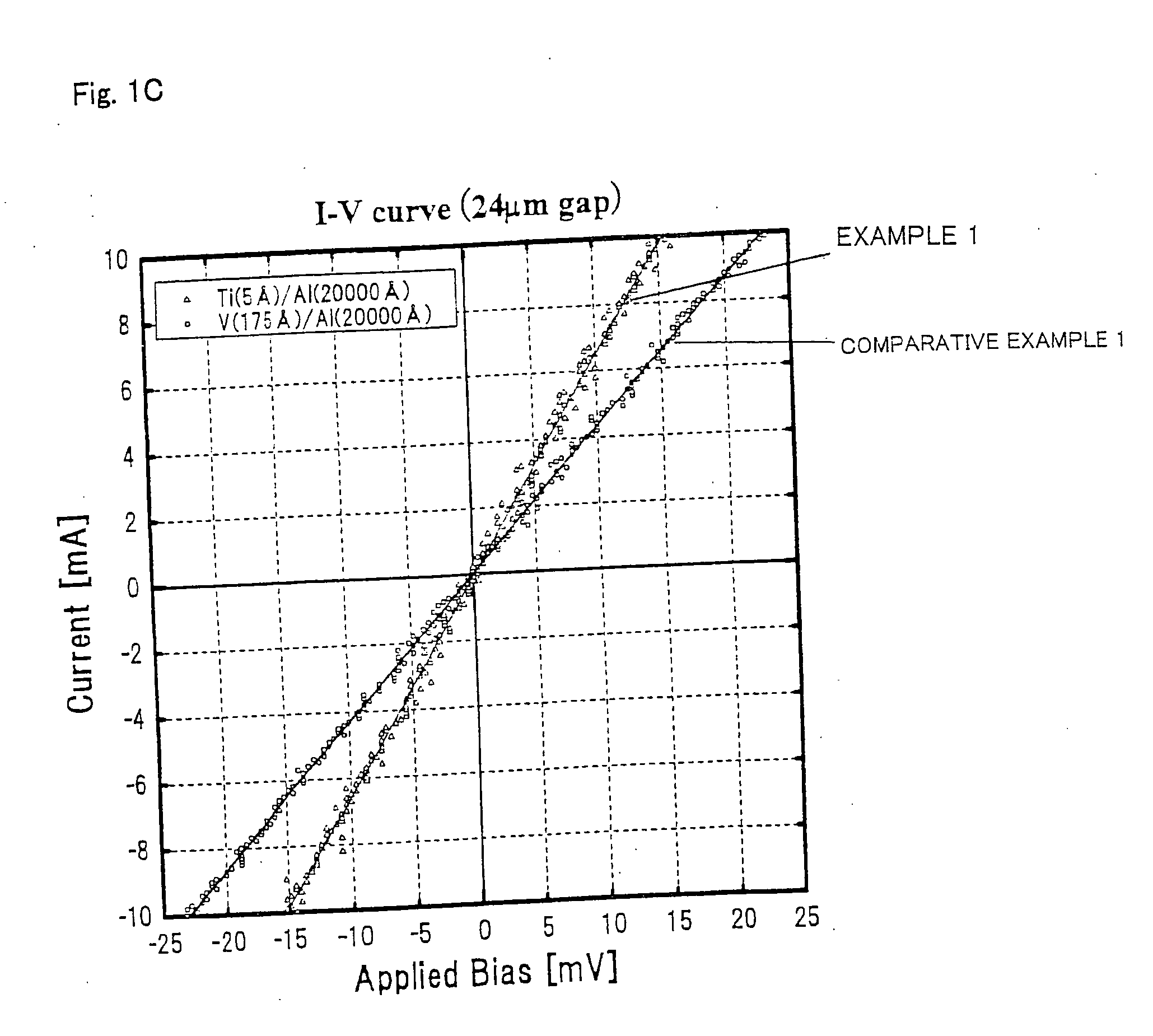
[0041]Electrodes according to the present invention were measured for contact resistance with respect to n-type GaN as described below.

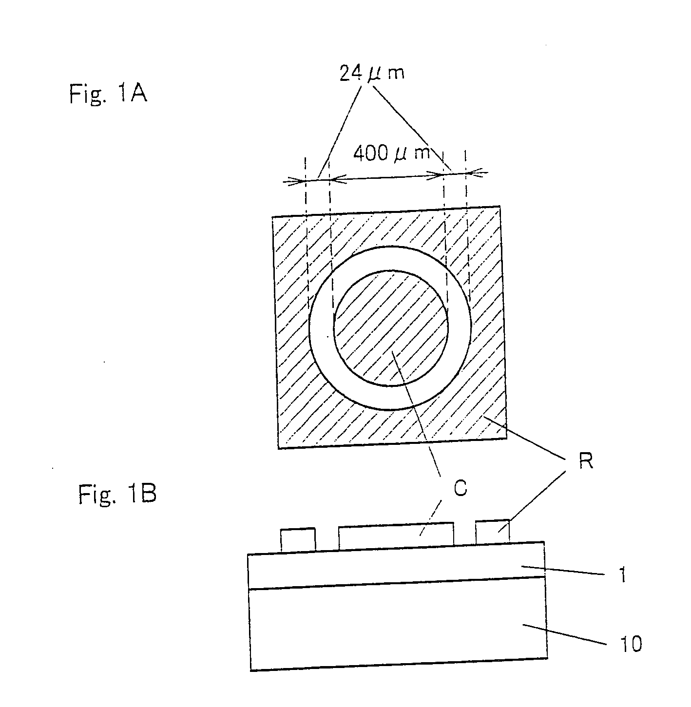
[0042]FIG. 1A is a plan view of a structure including a first electrode C and second electrode R measured for contact resistance. FIG. 1B is a sectional view of the structure. As shown in FIG. 1B, a buffer layer (not shown) made of aluminum nitride (AlN) was formed on a sapphire substrate 10. A layer of GaN was formed on the buffer layer by MOVPE so as to have a thickness of about 4 μm and then doped with Si at a dose of 4×1018 cm−3, whereby an n-type GaN layer 1 was formed. The first and second electrodes C and R were formed on the n-type GaN layer 1 by vacuum vapor deposition. The first and second electrodes C and R may be formed by a sputtering process.

[0043]As shown in FIG. 1A, the first electrode C was disk-shaped and had a diameter of 400 μm. The second electrode R was spaced from the first electrode C at a distance of 24 μm and was ring-shaped...

example 2

[0048]An electrode according to the present invention was evaluated for reflectivity by a method below.

[0049]A first sample including a first sapphire substrate with a thickness of 400 μm and a first electrode disposed thereon was prepared in such a manner that a titanium (Ti) layer with a thickness of 0.5 nm (5 Å) and a first aluminum (Al) layer with a thickness of 2 μm were deposited on the first sapphire substrate in that order (Example 2).

[0050]A second sample, including a second sapphire substrate with a thickness of 400 μm and a second electrode disposed thereon, for comparison was prepared in such a manner that a first vanadium (V) layer with a thickness of 17.5 nm (175 Å) and a second aluminum (Al) layer with a thickness of 2 μm were deposited on the second sapphire substrate in that order (Comparative Example 2).

[0051]A third sample, including a third sapphire substrate and a third electrode disposed thereon, for comparison was prepared in such a manner that a third aluminu...

example 3

[0063]Light-emitting devices were prepared and then evaluated as described below.

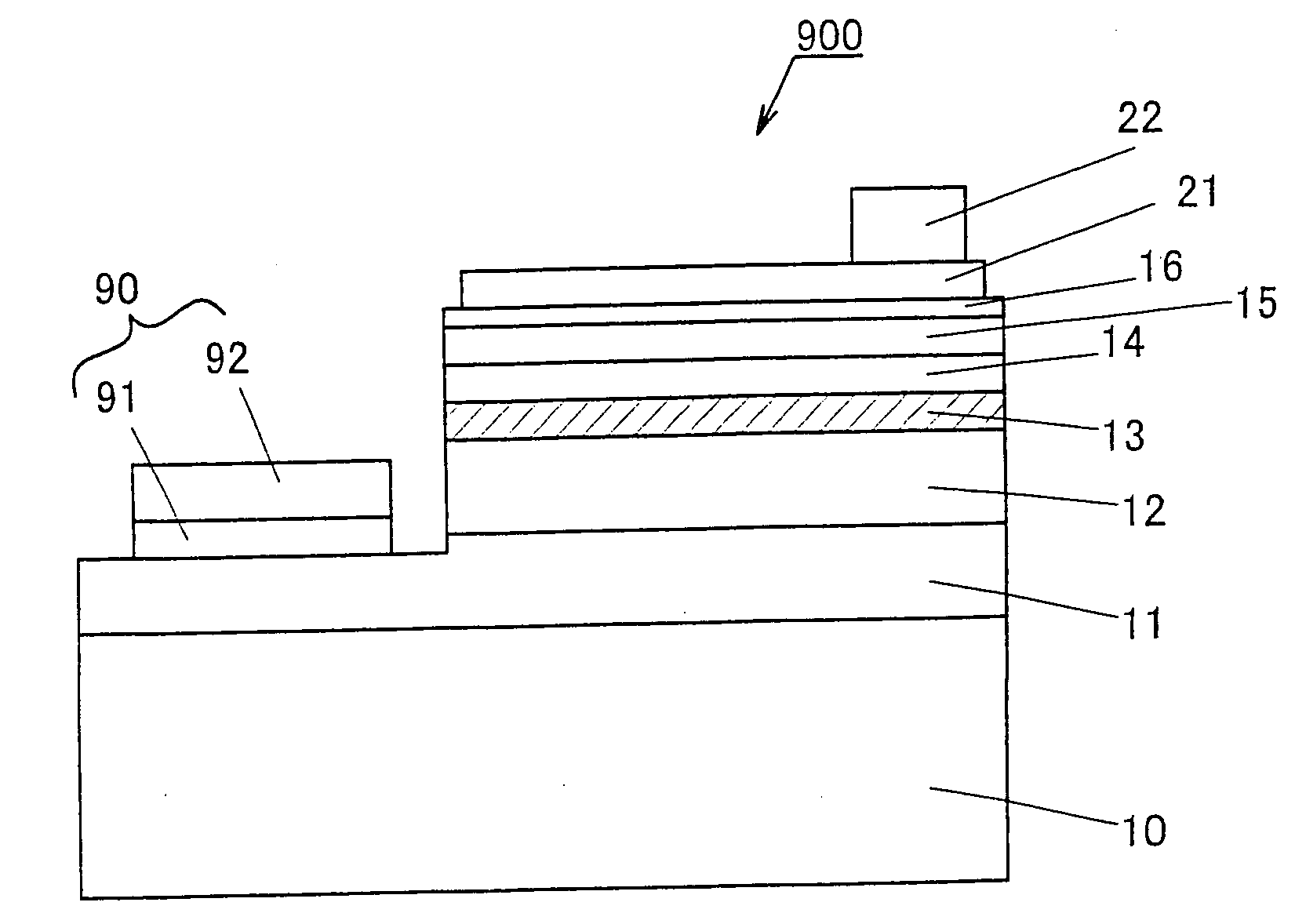
[0064]FIG. 3 is a sectional view of a first Group-III nitride compound semiconductor light-emitting device 100 according to an embodiment of the present invention. The first Group-III nitride compound semiconductor light-emitting device 100 includes a sapphire substrate 10, a buffer layer (not shown) made of aluminum nitride (AlN), an n-type GaN layer 11 doped with Si, an n-type AlGaN clad layer 12 doped with Si, a light-emitting layer 13 having a GaN / InGaN multi-quantum well structure, a p-type AlGaN clad layer 14 doped with Mg, a p-type GaN layer 15 doped with Mg, and a p+-type GaN layer 16, these layers being deposited on the sapphire substrate 10 by MOCVD or MOPVD in that order.

[0065]The first Group-III nitride compound semiconductor light-emitting device 100 further includes a translucent electrode 21, made of ITO, extending over the p+-type GaN layer 16; a pad electrode 22, made of gold, lying on ...


PUM

PropertyMeasurementUnit
thicknessaaaaaaaaaa
thicknessaaaaaaaaaa
reflectivityaaaaaaaaaa

Abstract

A method for forming an electrode for Group-III nitride compound semiconductor light-emitting devices includes a step of forming a first electrode layer having an average thickness of less than 1 nm on a Group-III nitride compound semiconductor layer, the first electrode layer being made of a material having high adhesion to the Group-III nitride compound semiconductor layer or low contact resistance with the Group-III nitride compound semiconductor layer and also includes a step of forming a second electrode layer made of a highly reflective metal material on the first electrode layer.

Description

BACKGROUND OF THE INVENTION[0001]1. Field of the Invention[0002]The present invention relates to a method for forming an electrode for Group-III nitride compound semiconductor light-emitting devices. The term “Group-III nitride compound semiconductor” used herein covers n- and p-type compound semiconductors doped with any element; compound semiconductors containing a Group-III or -V element and at least one selected from the group consisting of B, Ti, P, As, Sb, and Bi; and compound semiconductors represented by the formula AlxGayIn1-x-yN, wherein x, y, and x+y are zero to one.[0003]2. Description of the Related Art[0004]Conventional group-III nitride compound semiconductor light-emitting devices have low light extraction efficiency. The following documents disclose various techniques for forming electrodes from metals having high visible light reflectivity: Japanese Unexamined Patent Application Publication Nos. 2003-086843, 2004-179347, 2005-011857, and 2004-140052.[0005]A convent...

Claims


Application Information

Patent Timeline
Patent Type & Authority Applications(United States)
IPC IPC(8): H01L21/285H01L33/10H01L33/22H01L33/32H01L33/42
CPCH01L21/0254H01L21/0262H01L33/32H01L33/405H01S5/0425H01S5/32341
Inventor GOSHONOO, KOICHIMORIYAMA, MIKI
Owner TOYODA GOSEI CO LTD
Why Eureka
Try Eureka