Semiconductor device and method of manufacturing the same

a semiconductor device and semiconductor technology, applied in the field of semiconductor devices, can solve the problems of discharging heat from the semiconductor device, complicated configuration, operational stability of the semiconductor device, etc., and achieve the effect of reducing the length of the micro-strip line, maximizing the isolation of patterns, and reducing the cost of manufacturing

Inactive Publication Date: 2008-12-04
PANASONIC CORP
View PDF5 Cites 21 Cited by
  • Summary
  • Abstract
  • Description
  • Claims
  • Application Information

AI Technical Summary

Benefits of technology

[0033]The first circuit pattern is formed which has the function of the micro-strip line having a continuous shape of one of a spiral, a meander, and a curve on the first major surface, the second land is formed at the opposite position from the first circuit pattern with the substrate disposed between the patterns and has an area as large as or larger than the first circuit pattern, and the second land is connected to the ground potential of the circuit pattern on the first major surface via the through via of the substrate. With this configuration, the isolations of the patterns can be maximized by optimizing the area of the second land pattern, thereby achieving an effective solution to undesired oscillation (for example, self oscillation and parasitic oscillation).
[0034]Since the substrate is one of a silicon wafer and a GaAs (gallium arsenide) wafer, the substrate has a high dielectric constant of at least 10 and the length of the micro-strip line can be shortened in a high-frequency region, thereby reducing the size and manufacturing cost of the semiconductor device.

Problems solved by technology

For example, in PA modules for GSM cellular phones, a signal package includes a plurality of semiconductor elements corresponding to triple bands serving as usable frequency bands and includes a number of chip passive components such as a chip capacitor and a chip inductor for a circuit configuration between the elements, resulting in a complicated configuration (for example, see Japanese Patent Laid-Open No. 2006-041401).
Thus it is not possible to obtain an electromagnetic shielding effect when the operating frequency is a high frequency of at least several hundreds MHz, causing a problem in obtaining the operational stability of the semiconductor device.
Another problem is how to dissipate heat from the semiconductor device when the heat is liberated during the operation of the semiconductor device as in a power semiconductor.
Further, the use of the resin substrate 91 inevitably increases the manufacturing cost including the material cost.
An inductance component with such a large value formed on a surface of the semiconductor device causes a large chip size and inevitably increases the manufacturing cost including the material cost.
Further, when a plurality of inductance components are formed on a surface of a semiconductor device, the chip area is increased and it is difficult to obtain high-frequency isolation between the components, resulting in higher manufacturing cost and a deterioration of high frequency characteristics.

Method used


Image

  • Semiconductor device and method of manufacturing the same
  • Semiconductor device and method of manufacturing the same
  • Semiconductor device and method of manufacturing the same

Examples


first embodiment

[0066]The following will describe a semiconductor device and a method of manufacturing the same according to a first embodiment of the present invention.

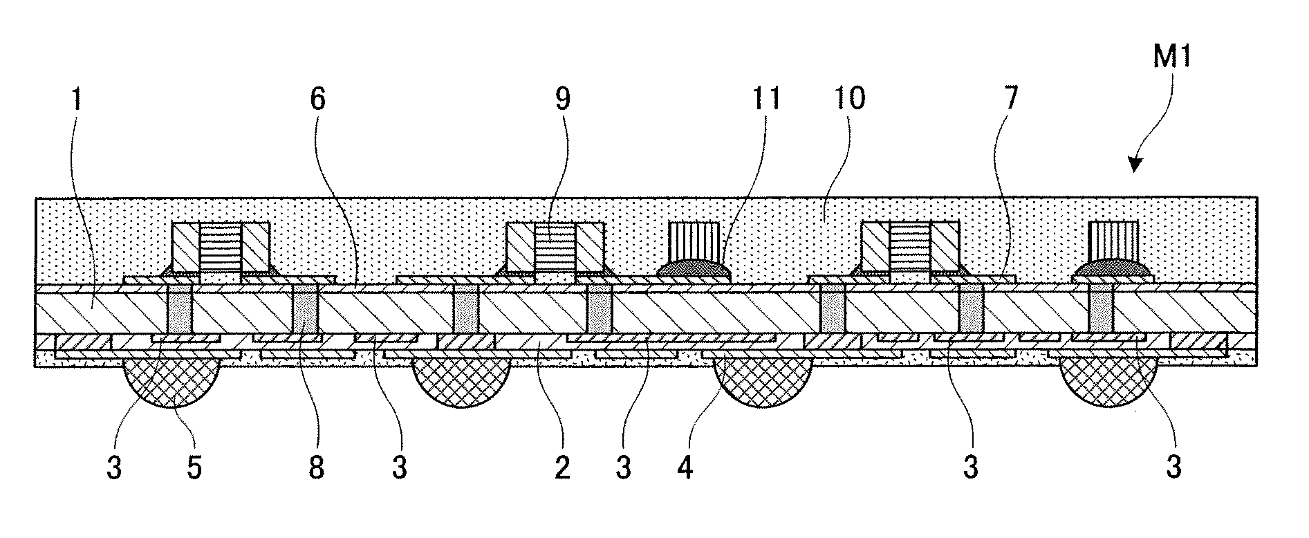
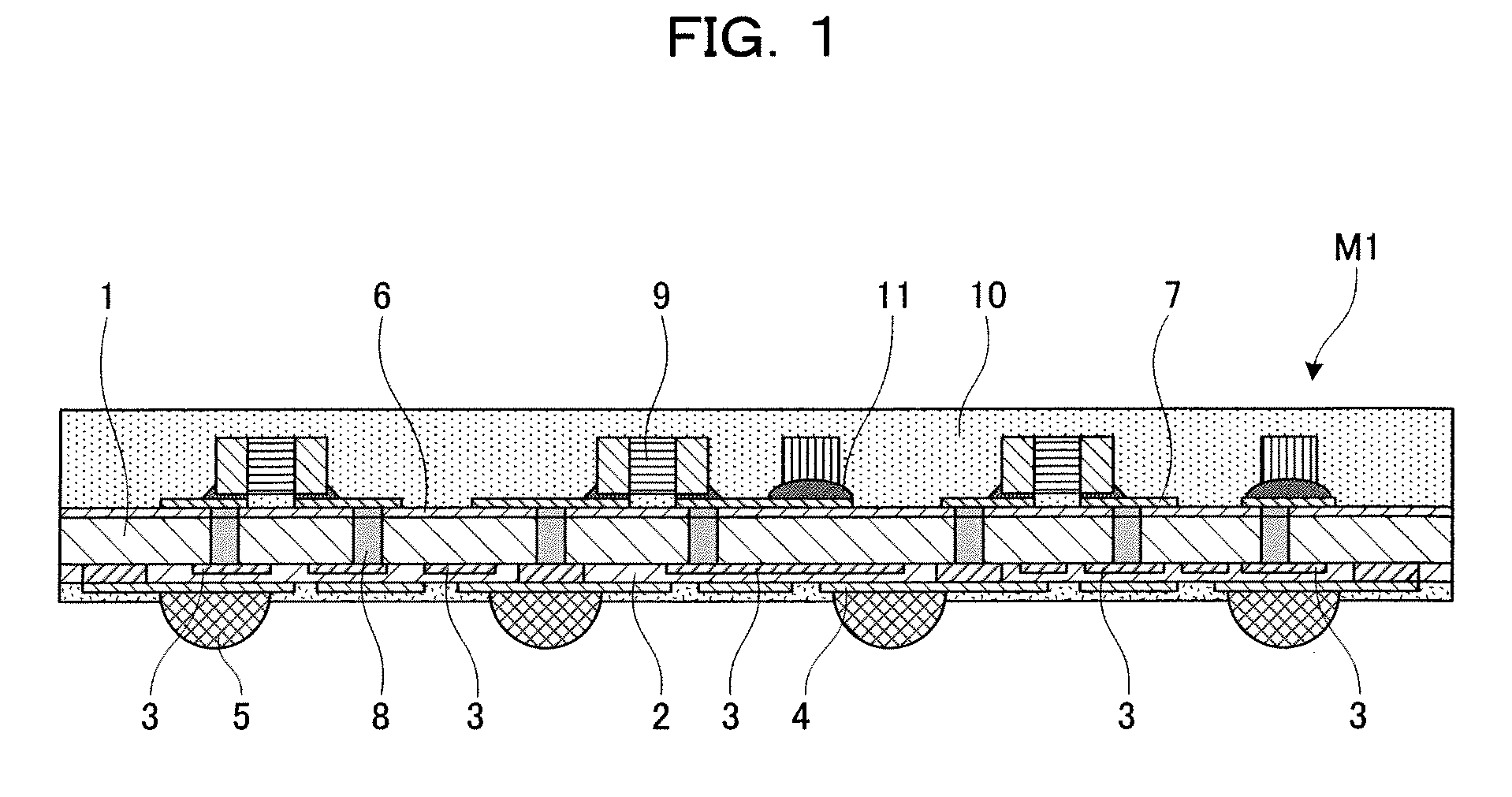
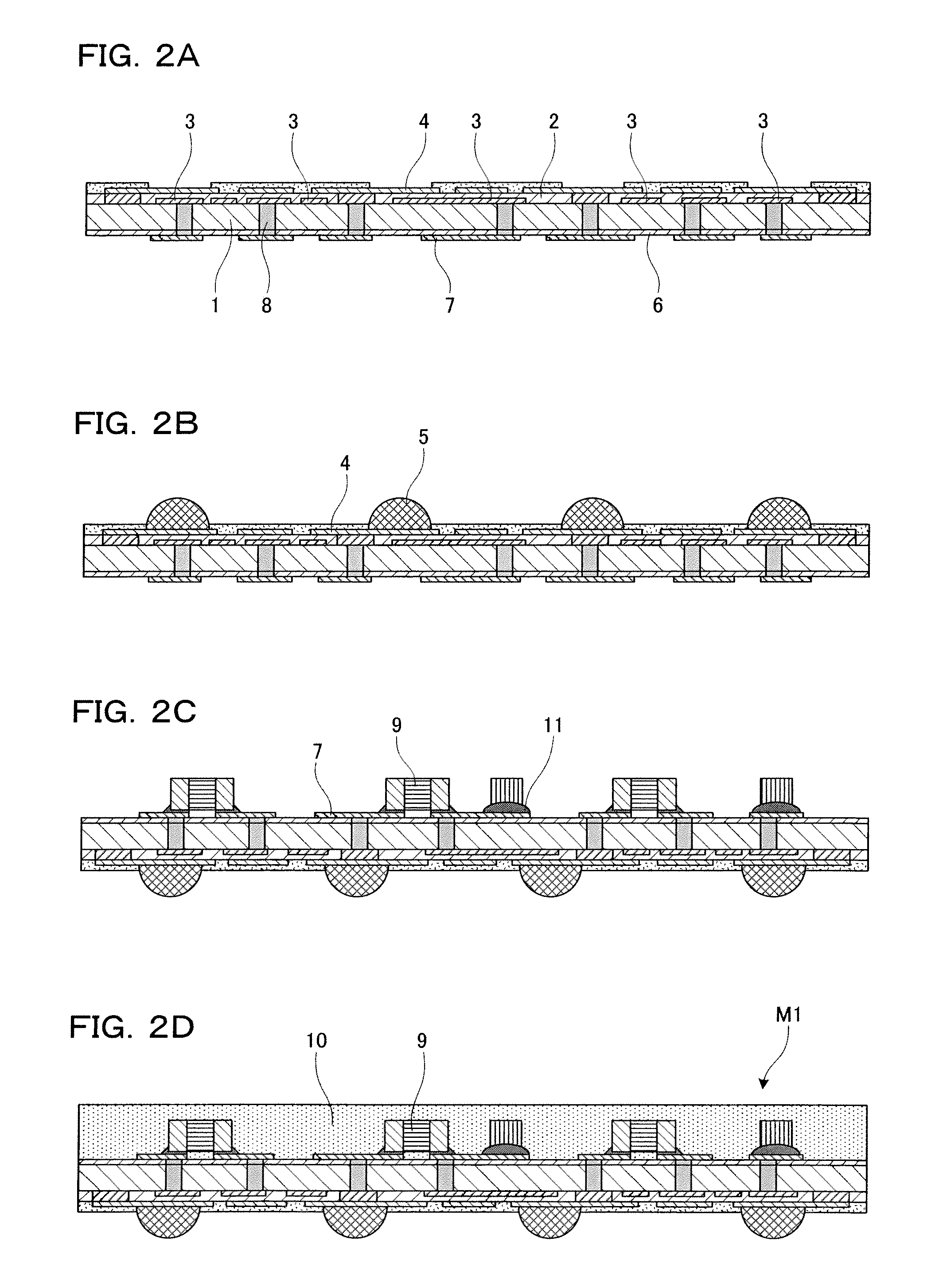
[0067]FIG. 1 is a sectional view showing the configuration of the semiconductor device according to the first embodiment. The semiconductor device of the sectional view is a power amplifier module for W-CDMA of 800 MHz to 2 GHz. In the semiconductor device of FIG. 1, a power amplifier module M1 is 5 mm high by 2.5 mm wide and is 1.1 mm thick. A substrate 1 is a GaAs (gallium arsenide) wafer. On the wafer surface layer (the lower part of FIG. 1) of the substrate 1, a semiconductor element made up of a power amplifier circuit pattern 3 is formed as a first circuit pattern. The substrate 1 is 0.25 mm thick. On the power amplifier circuit pattern 3, a first insulating layer 2 is formed which is made of epoxy resin and is 0.1 mm thick. Further, copper rewiring 4 and hemispherical solder electrodes 5 for external connection are formed the...

second embodiment

[0076]The following will describe a semiconductor device and a method of manufacturing the same according to a second embodiment of the present invention.

[0077]FIG. 3 is a sectional view schematically showing the configuration of the semiconductor device according to the second embodiment. In the semiconductor device of FIG. 3, a power amplifier module M1 is 5 mm high by 2.5 mm wide and is 1.1 mm thick. A substrate 1 is a GaAs wafer. On the wafer surface layer (the lower part of FIG. 3) of the substrate 1, a semiconductor element made up of a power amplifier circuit pattern 3 is formed as a first circuit pattern. The substrate 1 is 0.25 mm thick. On the power amplifier circuit pattern 3, a first insulating layer 2 is formed which is made of epoxy resin and is 100 μm thick. Further, copper rewiring 4 and solder electrodes 5 for external connection are formed thereon.

[0078]The solder electrodes 5 are formed using hemispherical Sn—Ag solder and Sn—Ag—Cu solder. The solder electrodes 5 ...

third embodiment

[0089]The following will describe a semiconductor device and a method of manufacturing the same according to a third embodiment of the present invention.

[0090]FIG. 5 is a sectional view schematically showing the configuration of the semiconductor device according to the third embodiment of the present invention. In the semiconductor device of FIG. 5, a power amplifier module M1 is 5 mm high by 2.5 mm wide and is 1.2 mm thick. A substrate 1 is a GaAs wafer. On the wafer surface layer (the lower part of FIG. 5) of the substrate 1, a semiconductor element made up of a power amplifier circuit pattern 3 is formed as a first circuit pattern. The substrate 1 is 0.25 mm thick. On the power amplifier circuit pattern 3, a first insulating layer 2 is formed which is made of epoxy resin and is 0.1 mm thick. Further, copper rewiring 4 and hemispherical solder electrodes 5 for external connection are formed thereon.

[0091]Conventionally, Sn—Pb eutectic solder has been used for the solder electrode...


PUM


Abstract

In the present invention, a first circuit pattern 3 composing a semiconductor element is formed on the front side of a substrate 1, a first insulating layer 2 is formed on the first circuit pattern 3, solder electrodes 5 for external connection are formed on the first insulating layer 2, a second insulating layer 6 is formed on the backside of the substrate 1, a second circuit pattern 7 is formed on the second insulating layer 6, through vias 8 are formed to connect the first circuit pattern 3 and the second circuit pattern 7, chip passive components 9 are placed on the second circuit pattern 7, and the backside of the substrate is integrally molded with epoxy resin 10 such that the epoxy resin 10 covers the chip passive components 9.

Description

FIELD OF THE INVENTION [0001]The present invention relates to a semiconductor device in which a circuit pattern and solder electrodes are formed on a substrate and the substrate is molded with resin such that the resin covers chip passive components placed on the circuit pattern, and a method of manufacturing the same.BACKGROUND OF THE INVENTION [0002]In recent years, particularly in the field of mobile communications mainly through cellular phones, the need for higher functionality has increased as well as the size reduction and slimming down of semiconductor devices for communications. Conventionally, a plurality of semiconductor elements have been used to configure a circuit on the substrate of a cellular phone. Thus there is a growing demand for advanced modules in which a plurality of semiconductor elements are stored in a single package and chip passive components such as a chip capacitor and a chip inductor are mounted in the package to provide a self-contained circuit and fu...

Claims


Application Information

Patent Timeline
Patent Type & Authority Applications(United States)
IPC IPC(8): H01L23/538H01L21/56
CPCH01L23/3114H01L23/4334H01L23/481H01L23/5227H01L23/642H01L23/645H01L25/16H01L2224/48227H01L2224/73265H01L2924/01078H01L2924/01079H01L2924/15311H01L2924/19041H01L2924/19104H01L2924/19105H01L2924/30107H01L2924/3011H01L2924/3025H05K1/023H05K1/0306H05K1/141H05K1/165H05K3/3436H05K2203/1316H01L24/48H01L2924/01322H01L2224/32225H01L2924/00H01L2924/00012H01L2924/10253H01L24/73H01L2924/00014H01L2924/181H01L2224/45099H01L2224/45015H01L2924/207
Inventor TAKEHARA, HIDEKITATEOKA, KAZUKI
Owner PANASONIC CORP
Why Eureka
Try Eureka