

Formation of nitride-based optoelectronic and electronic device structures on lattice-matched substrates
a technology of optoelectronic and electronic devices, applied in semiconductor/solid-state device manufacturing, semiconductor devices, electrical equipment, etc., can solve the problems of reducing the performance impact of dislocation defects on the active regions, affecting device performance, etc., and achieve high epitaxial layer quality
- Summary
- Abstract
- Description
- Claims
- Application Information
AI Technical Summary
Benefits of technology
Problems solved by technology
Method used
Image

Examples
example 1
UV LED Grown on GaN Substrate and Substrate Removal by Grinding
[0069]A UV LED may be made by epitaxially growing AlxGayN (where 0≦x≦1, 0≦y≦1 and x+y=1) layer(s) on a low dislocation density GaN substrate, with grading from GaN to AlGaN, to form a semiconductor device complex. The stoichiometry of the AlxGayN alloy is chosen to be consistent with the wavelength of the emitter. Subsequently, the GaN may be ground away until the AlInGaN layer is reached. The resulting device, devoid of the GaN substrate, is an optoelectronic device structure useful as an UV LED.
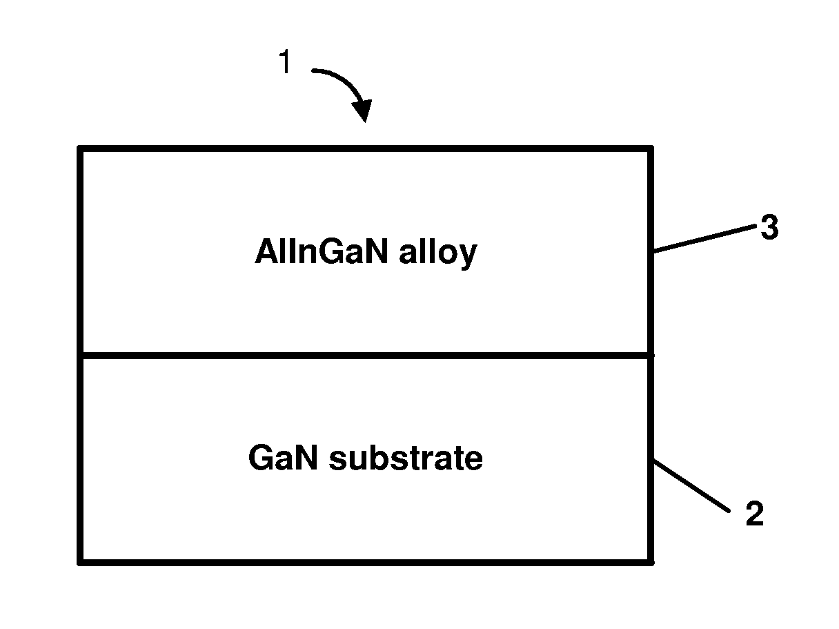
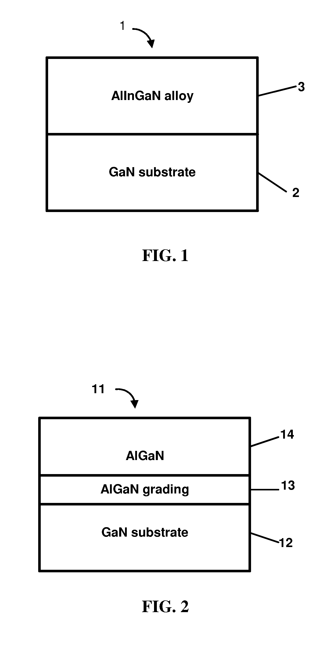
[0070]An illustration of a schematic cross-sectional view of a first semiconductor device complex, prior to removal of the GaN substrate, is set forth in FIG. 2. Specifically, the semiconductor device complex 11 comprises a low dislocation density gallium nitride substrate 12, an AlGaN grading layer 13, and at least one AlGaN epitaxial layer 14, which forms the active region of the electronic or optoelectronic device structure.
example 2
UV LED Grown on GaN Substrate and Substrate Removal by Photon Exposure
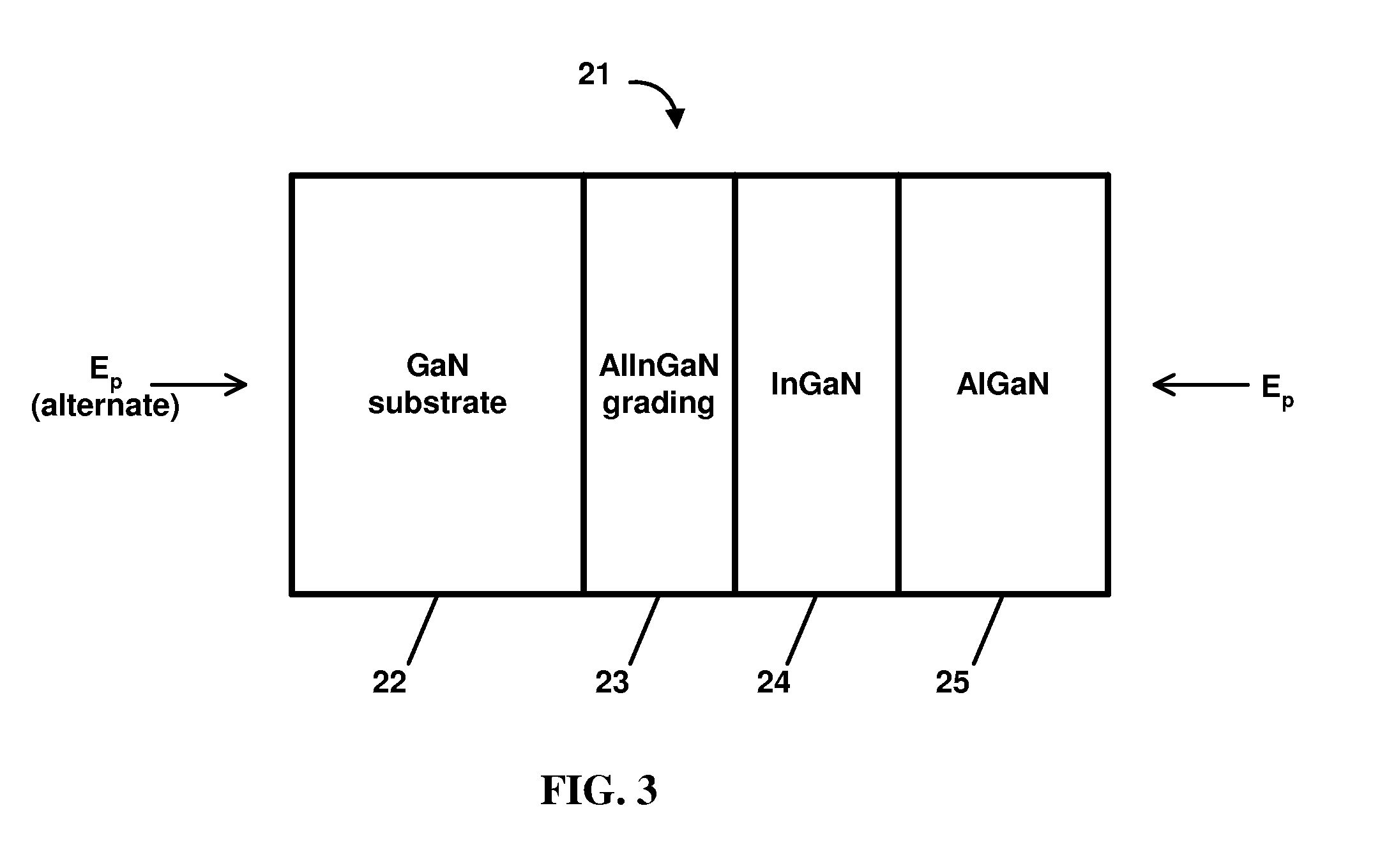
[0071]A UV LED may be made by epitaxially growing AlxGa1-xN layer(s) on a low dislocation density GaN substrate with an AlInGaN grading layer and an InGaN parting layer to form a semiconductor device complex. Subsequently, the complex is exposed to photons, from the front or the rear of the structure. If a carrier wafer is being used on top of the AlGaN layers, then illumination with photons must precede attachment with the carrier wafer or the carrier wafer must be transparent to the photons. Alternatively, photon exposure may be from the back of the complex, provided that the parting layer has a bandgap less than the substrate and grading layers (as in the case of a GaN substrate and an InGaN parting layer). The photons are absorbed by the InGaN parting layer, but not the GaN substrate or AlInGaN grading layers, causing separation of the GaN substrate and LED device structure at the InGaN parting layer.
[0072]An ...
example 3
UV LED Grown on GaN Substrate and Substrate Removal by Ion Implantation and RTA
[0073]A UV LED may be made by epitaxially growing AlInGaN alloy layer(s) on a low dislocation density GaN substrate with an AlGaN grading layer to form a semiconductor device complex. The complex may be subsequently bombarded with monoenergetic H+ ions to implant such ions in the complex at a predetermined depth in the AlGaN layer. A carrier may be optionally added to the top of the epitaxial layer(s) of the semiconductor device complex. RTA may be used to fracture the complex along the line of the mean H+ implant depth, allowing removal of the GaN substrate from the LED. The backside of the LED may be cleaned and roughened and mounted to a substrate, if desired. The attached substrate is different from that on which the LED was grown. Once mounted, the LED and attached substrate may be annealed to remove any damage from the previous processes. The removed GaN substrate may be polished and reused for addi...
PUM
 Abstract
Description
Claims
Application Information