Method of Aligning Optical Components With Waveguides

a waveguide and optical component technology, applied in the direction of optical waveguide light guide, instruments, electrical equipment, etc., can solve the problems of increasing the susceptibility of the alignment process, limiting the vertical evanescent coupling of components, and preventing the straightforward integration of non-waveguide components such as free space optical isolators and thin film filters, so as to reduce the sensitivity of the placement of a hybrid optical component to dust and other contamination on the waveguide surfa

Active Publication Date: 2008-12-18
HUAWEI TECH CO LTD
View PDF6 Cites 40 Cited by
  • Summary
  • Abstract
  • Description
  • Claims
  • Application Information

AI Technical Summary

Benefits of technology

[0015]Thus, the invention, at least in the preferred embodiments, provides a technique which allows the surface of a cladding layer containing bumps to be used as a vertical reference frame for passive alignment that does not r

Problems solved by technology

This approach is limited to vertical evanescent coupling of components and precludes the straightforward integration of non-waveguiding components such as free space optical isolators and thin film filters.
In reality, however, the top surface of a cladding over waveguides may not always be planar and in some situations the cladding surface of the waveguide device may have undulations or bumps above the regions which define the waveguide core.
In ad

Method used


Image

  • Method of Aligning Optical Components With Waveguides
  • Method of Aligning Optical Components With Waveguides
  • Method of Aligning Optical Components With Waveguides

Examples


Embodiment Construction

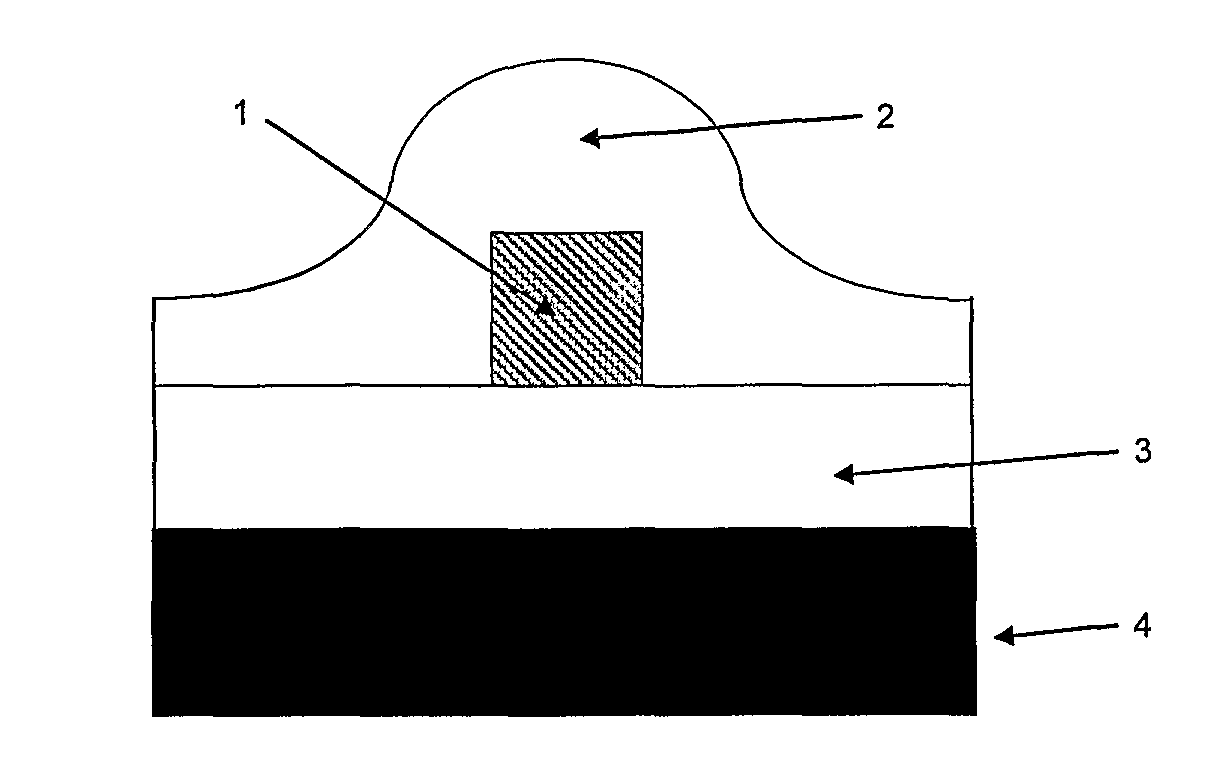
[0024]Square (or rectangular) waveguide cross sections are common in planar waveguide devices, where the core cross section can have linear dimensions of the order of a few to several microns in each direction for single mode operation. FIG. 1 shows a typical configuration of such a planar waveguide device. The waveguide core 1 sits on a buffer layer 3 formed of a material of lower refractive index than the waveguide core 1. The buffer layer 3, in turn, sits on a suitable substrate 4. Typically, the waveguide core 1 is applied to the buffer layer 3 as a continuous layer and portions of the waveguide material are removed, for example by etching, to leave a pattern of core material. For this reason, the each waveguide core has the same height above the buffer layer 3.

[0025]A uniform thickness of cladding layer 2 is deposited on top of the waveguide core 1 (using one of a number of possible deposition techniques). The cladding layer 2 is substantially planar in regions that do not cont...


PUM


Abstract

A method of fabricating a photonic device comprises the steps of providing a core pattern of waveguide core material (1) on a base layer (3) and applying a cladding layer (2) over the core material 1 and the base layer (3). The height of the surface of the cladding layer (2) over the base layer (3) varies in dependence on the pattern of core material (1). The core pattern is designed with at least two reference regions, each having a width w that is selected to provide a peak of the cladding layer (2) with a predetermined height hl over each reference region. The core pattern is further designed such that a line between the peaks of the reference regions is higher than any intervening peaks of the cladding layer, whereby the peaks of the reference regions provide a vertical alignment reference.

Description

FIELD OF THE INVENTION [0001]This invention relates to a method of fabricating a photonic device including at least one waveguide, and in particular to a method of aligning optical components with waveguides.BACKGROUND OF THE INVENTION [0002]There are approaches used for passive hybrid assembly of semiconductor optical components with planar waveguides, such as that used by Blauvelt in U.S. patent application US2004 / 0052467 that uses evanescent (vertical in this case) coupling to an underlying passive waveguide wafer. This approach is limited to vertical evanescent coupling of components and precludes the straightforward integration of non-waveguiding components such as free space optical isolators and thin film filters. In addition, the alignment technique means that the cladding layer of the waveguide wafer has to be both very thin to enable the evanescent coupling to take place and substantially flat.[0003]An alternative is that disclosed by Maxwell in U.S. Pat. No. 6,778,718 rel...

Claims


Application Information

Patent Timeline
IPC IPC(8): H01L21/02G02B6/122G02B6/13G02B6/30G02B6/42
CPCG02B6/122G02B6/13G02B6/30G02B6/423
Inventor MAXWELL, GRAEME DOUGLASTOWNLEY, PHILIP RICHARDMCDOUGALL, ROBERT CAMPBELL
Owner HUAWEI TECH CO LTD
Why Eureka
Try Eureka