Semiconductor device

a semiconductor and device technology, applied in the field of objects, can solve the problems of inability to achieve mobility which is necessary and sufficient, inability to achieve mobility, and inability to achieve high speed operation, etc., and achieve the effects of low cost, high speed and low power

Active Publication Date: 2009-01-01
SEMICON ENERGY LAB CO LTD
View PDF99 Cites 384 Cited by
  • Summary
  • Abstract
  • Description
  • Claims
  • Application Information

AI Technical Summary

Benefits of technology

[0092]A semiconductor device can be manufactured with low cost. Alternatively, a multifunctional semiconductor device can be provided. Alternatively, a semiconductor device provided with a circuit which can operate at high speed can be provided. Alternatively, a semiconductor device which consumes low power can be provided. Alternatively, a semiconductor device of which manufacturing steps are reduced can be provided.

Problems solved by technology

However, even in a case where microcrystalline silicon or polycrystalline silicon as well as amorphous silicon is used, there is a problem in that characteristics thereof are incomparable to characteristics of single-crystal silicon.
In particular, in a semiconductor layer which is used for a conventional panel where a driver circuit is integrated, mobility which is necessary and sufficient is not obtained.
This has caused a big problem in manufacturing a semiconductor device of which high speed operation is required, that is, a driver circuit.

Method used


Image

  • Semiconductor device
  • Semiconductor device
  • Semiconductor device

Examples


embodiment modes

[0133]Embodiment Modes of the present invention will be hereinafter described in detail with reference to the accompanying drawings. However, it is easily understood by those skilled in the art that the present invention can be implemented in various different modes, and modes and details of the present invention can be modified in various ways without departing from the purpose and the scope of the present invention. Accordingly, the present invention should not be interpreted as being limited to the description of the embodiment modes. Note that in structures of the present invention described below, reference numerals denoting the same components are used in common in different drawings, and detailed description of the same portions or portions having similar functions is omitted.

embodiment mode 1

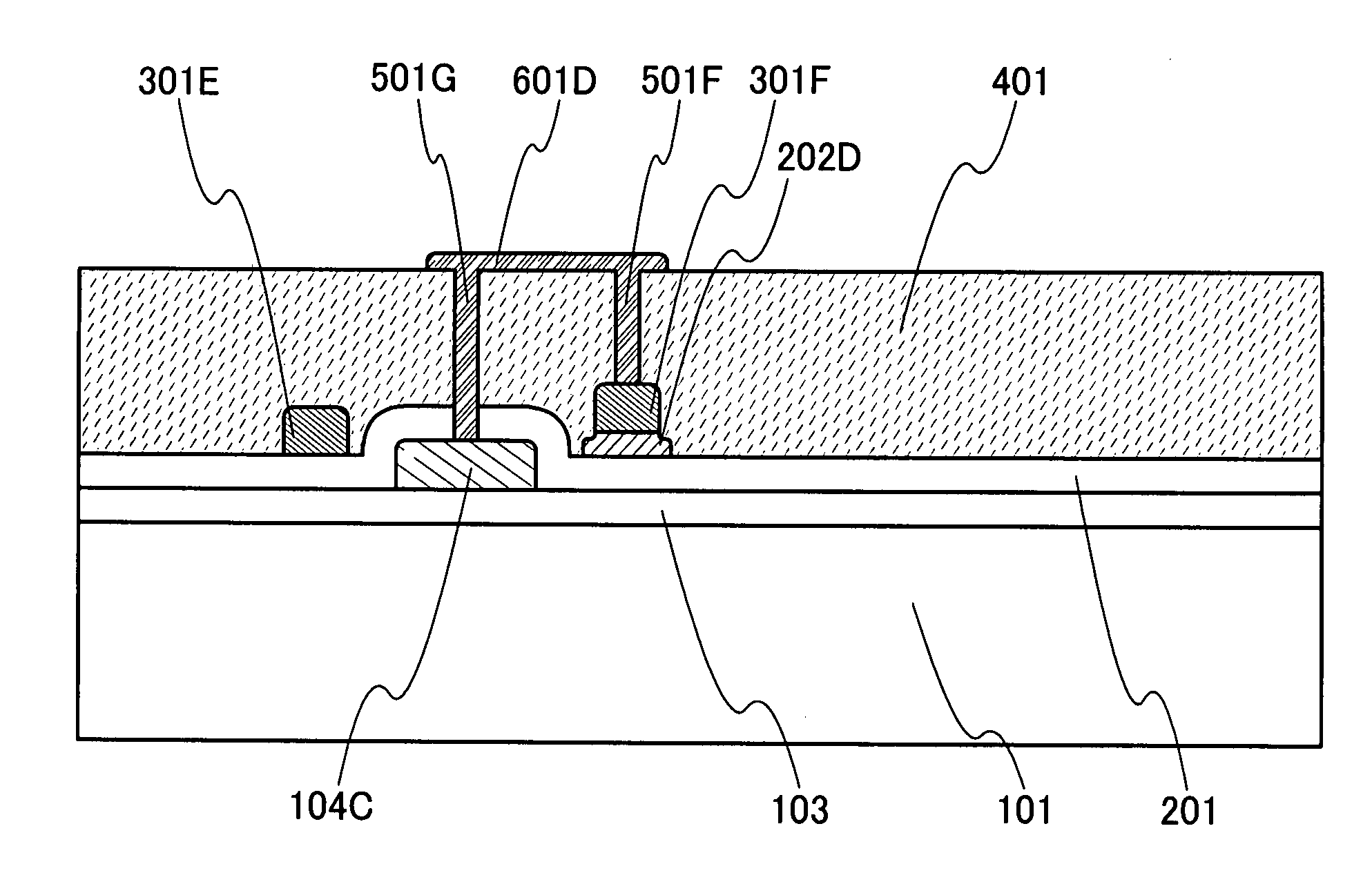
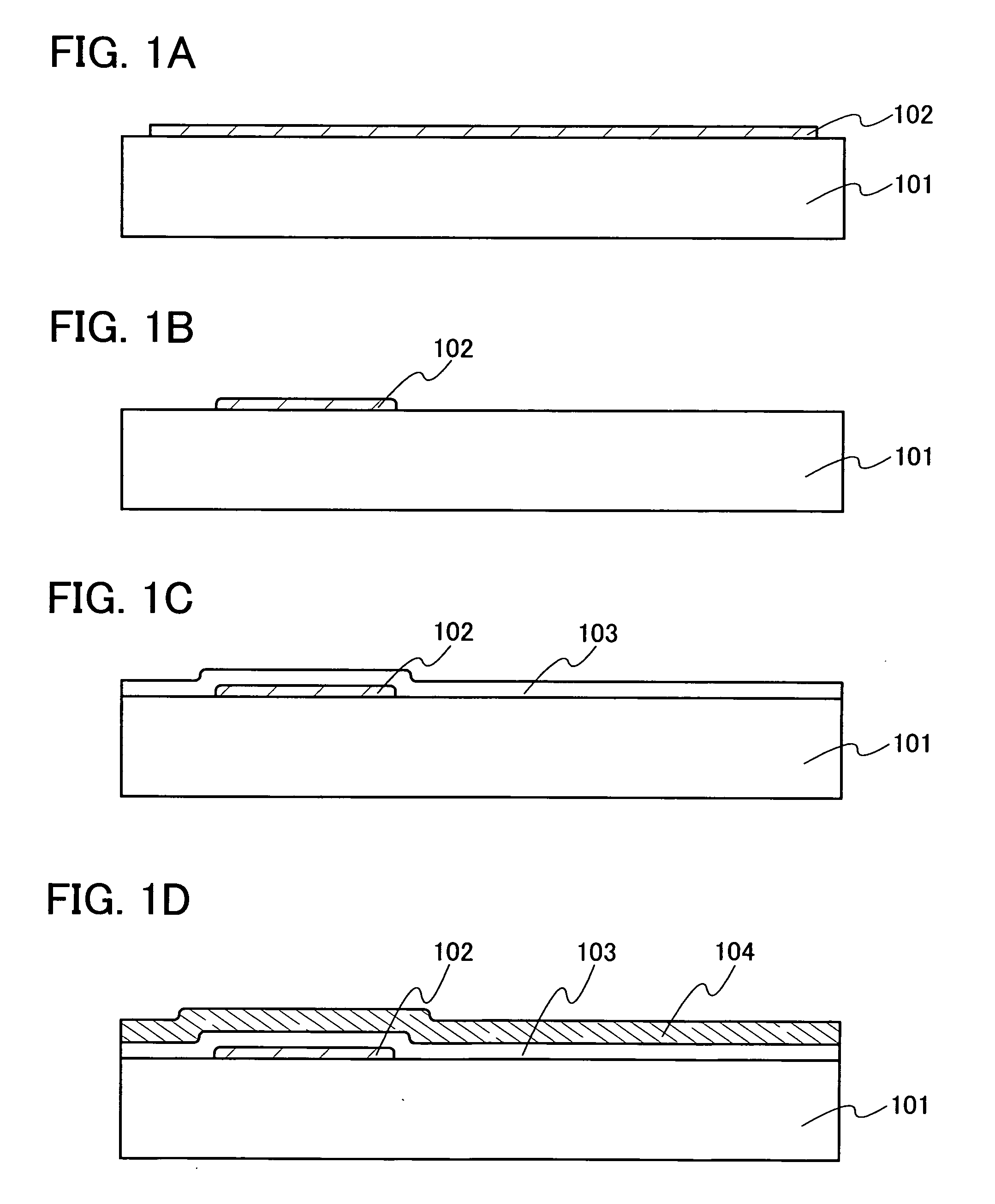
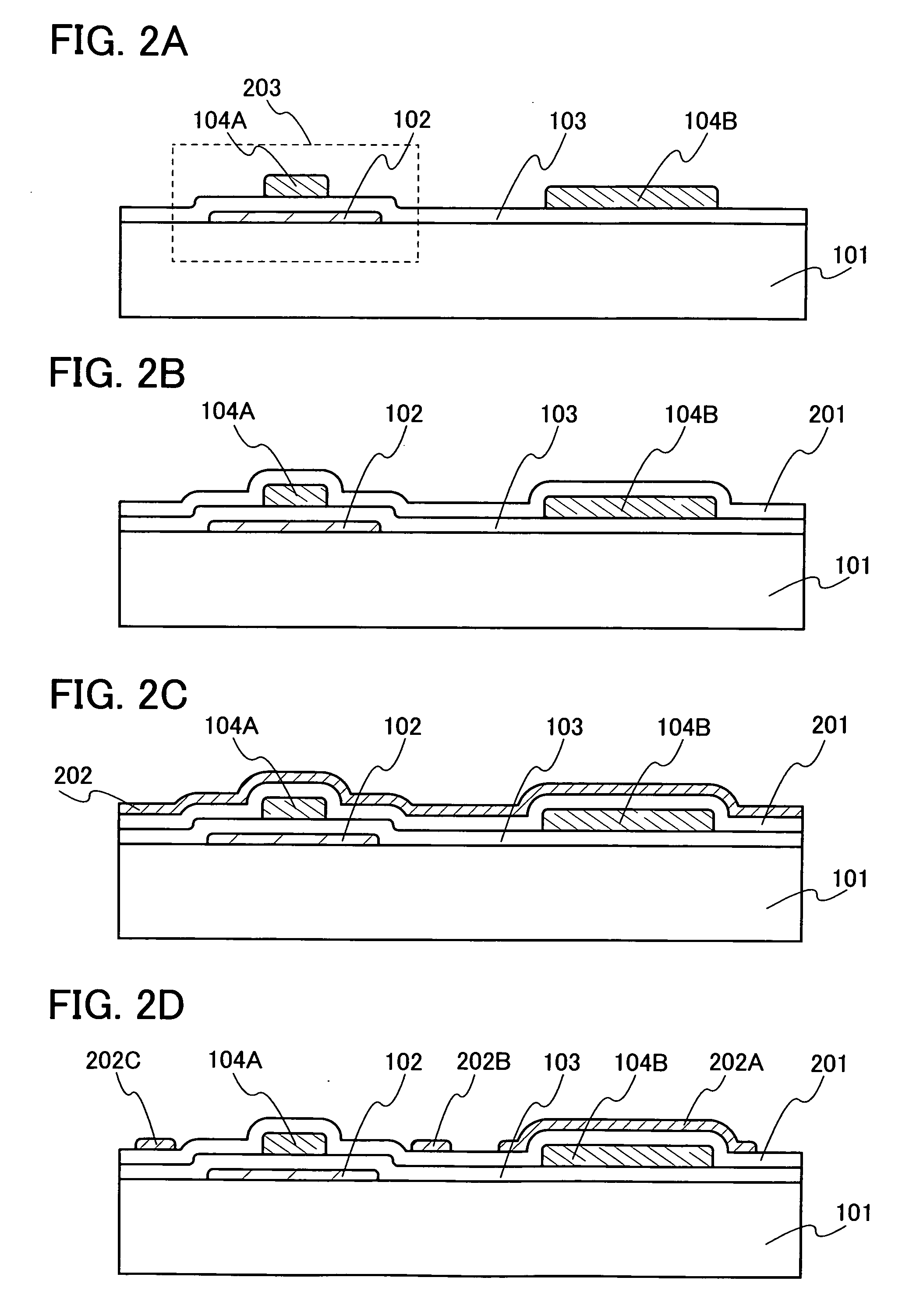
[0134]All or a part of a semiconductor device or a display device includes a TFT which is formed over a glass substrate in such manner that a silicon layer is separated from a single-crystal substrate and bonded (transferred) to the glass substrate, or a TFT formed over a glass substrate in such a manner that a single-crystal substrate is bonded to the glass substrate and separated from the glass substrate to form a silicon layer over the glass substrate. Not that the TFTs which is formed over a glass substrate in such manner that a silicon layer is separated from a single-crystal substrate and transferred to the glass substrate, or a TFT formed over a glass substrate in such a manner that a single-crystal substrate is bonded to a glass substrate and separated from the glass substrate to transfer a silicon layer which is part of the silicon substrate over the glass substrate are hereinafter referred to as single-crystal TFT.

[0135]Then, a non-single-crystal TFT is also formed at the ...

embodiment mode 2

[0210]Next, an arranging method of the semiconductor layer used for the single-crystal TFT is described.

[0211]FIGS. 12A and 12B show an SOI substrate of the present invention. In FIG. 12A, a base substrate 9200 is a substrate having an insulating surface or an insulating substrate, and a variety of glass substrates that are used in the electronics industry, such as aluminosilicate glass, aluminoborosilicate glass, or barium borosilicate glass, can be used. Alternatively, a quartz glass substrate or a semiconductor substrate such as a silicon wafer can be used. An SOI layer 9202 is a single-crystal semiconductor, and single-crystal silicon is typically applied thereto. Alternatively, a semiconductor layer which is separated from a single-crystal semiconductor layer or a polycrystal semiconductor layer of silicon or germanium using a hydrogen ion implantation separation method can be applied. Alternatively, crystalline semiconductor layer formed by using a compound semiconductor such ...


PUM

PropertyMeasurementUnit
temperatureaaaaaaaaaa
thicknessaaaaaaaaaa
thicknessaaaaaaaaaa

Abstract

It is an object to provide a semiconductor device which has a large size and operates at high speed. A top gate transistor which includes a semiconductor layer of single-crystal and a bottom gate transistor which includes a semiconductor layer of amorphous silicon (microcrystalline silicon) are formed over the same substrate. Then, gate electrodes of each transistor are formed with the same layer, and source and drain electrodes are also formed with the same layer. Thus, manufacturing steps are reduced. In other words, two types of transistors can be manufactured by adding only a few steps to the manufacturing process of a bottom gate transistor.

Description

BACKGROUND OF THE INVENTION[0001]1. Field of the Invention[0002]The present invention relates to an object, a method, or a method for producing an object. The present invention relates to a display device or a semiconductor device, in particular. The present invention relates to a display device or a semiconductor device which is formed by single-crystal being transferred to a glass substrate, in particular.[0003]2. Description of the Related Art[0004]In recent years, flat panel displays such as liquid crystal display devices and electroluminescence (EL) display devices have attracted attention.[0005]Driving methods of the flat panel displays include a passive matrix method and an active matrix method. An active matrix method has advantages over a passive matrix method such as the facts that power consumption is lowered, definition is heightened, a larger substrate can be used, and the like.[0006]In a structure where a driver circuit is provided outside the panel, it is possible to ...

Claims


Application Information

Patent Timeline
Patent Type & Authority Applications(United States)
IPC IPC(8): G02F1/136H01L29/04H01L21/84
CPCH01L27/1214H01L27/1292H01L27/1266H01L27/1251
Inventor KIMURA, HAJIME
Owner SEMICON ENERGY LAB CO LTD
Why Eureka
Try Eureka