

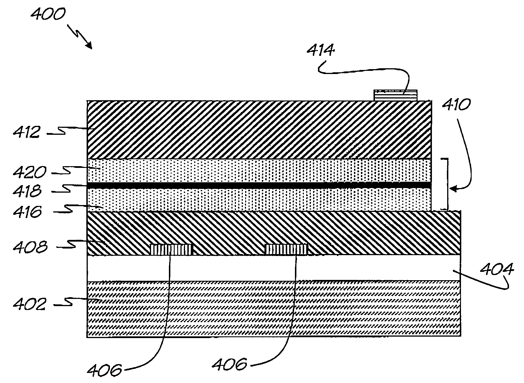
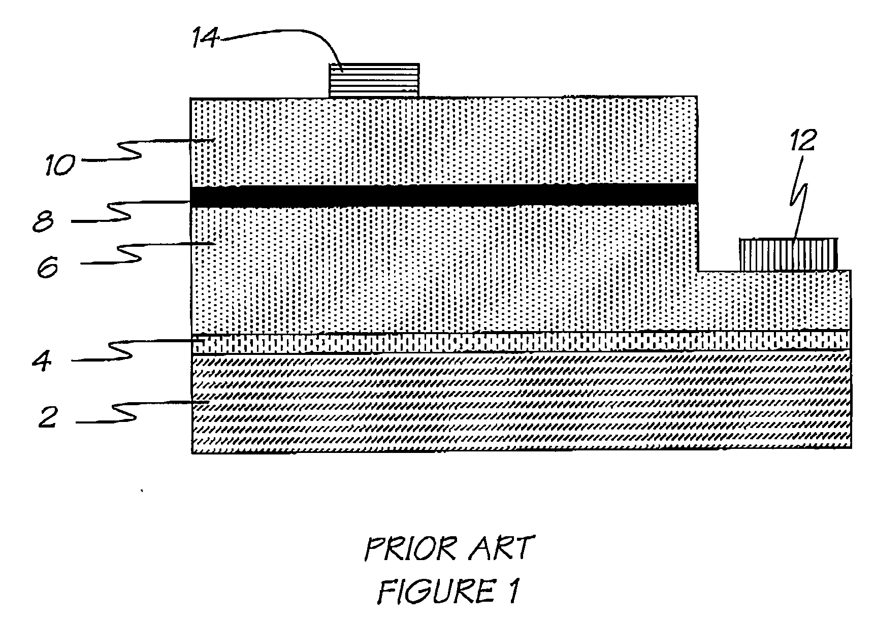
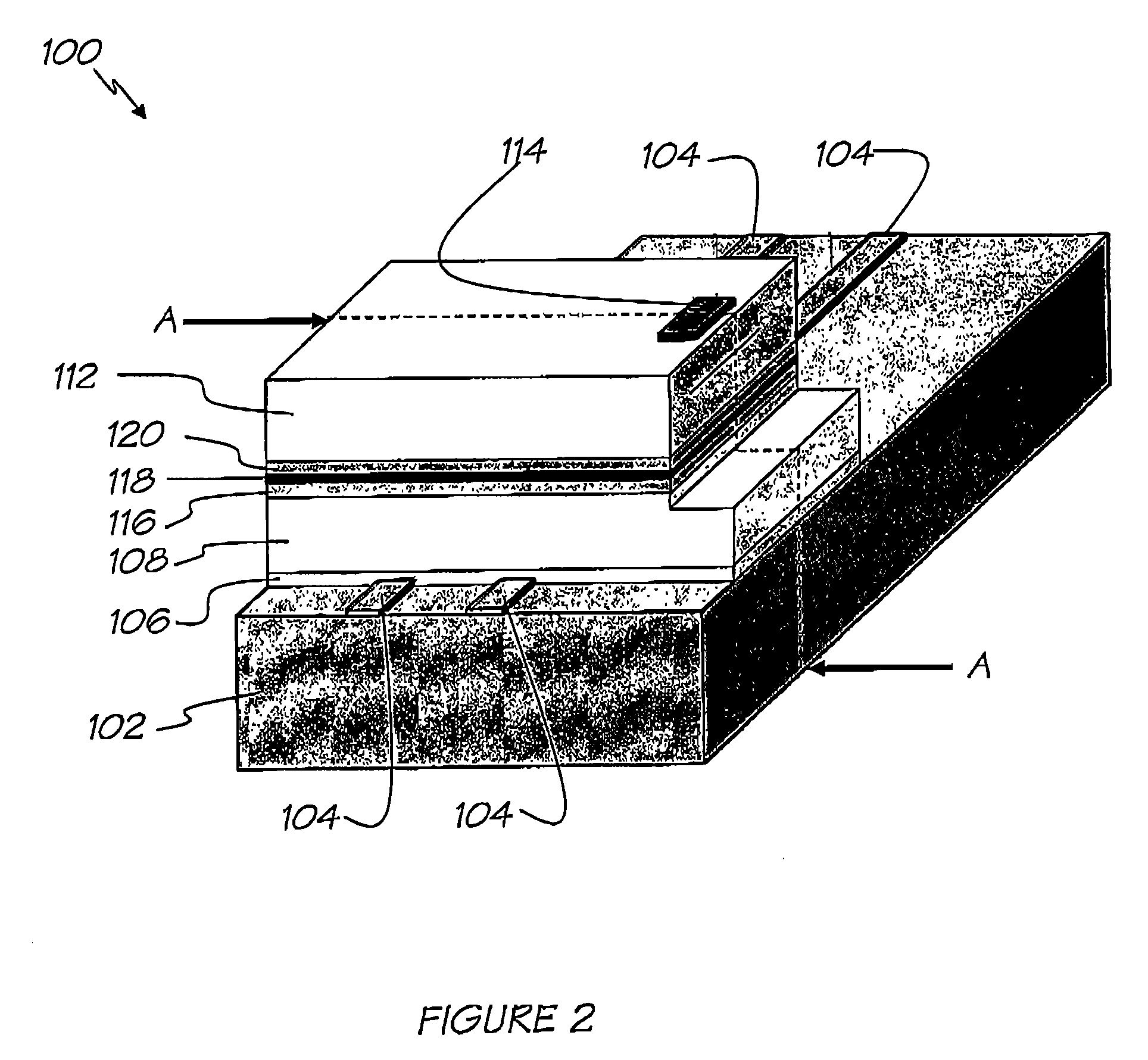
Buried contact devices for nitride-based films and manufacture thereof
- Summary
- Abstract
- Description
- Claims
- Application Information
AI Technical Summary
Benefits of technology
Problems solved by technology
Method used
Image

Examples
example
[0211]Gallium nitride devices on metal have been grown on sapphire substrates using the RPECVD method described above. In one example, a double heterostructure junction device comprising 5 layers has been demonstrated. The device was grown on a sapphire substrate which had a contact layer of nichrome deposited on the surface of the substrate prior to being placed in the RPECVD growth chamber. Nichrome is an alloy of nickel and chromium with high electrical resistance and an ability to withstand high temperatures.
[0212]An n-type GaN layer was grown at 541° C. for four hours on the nichrome layer at a reactor pressure of about 1.3 Torr. The precursor for the n-type GaN layer was delivered to the sample by flowing nitrogen through trimethylgallium (TMG) being held at −10° C. at a rate of 20 sccm (standard cubic centimetres per minute). Nitrogen was flowed through the plasma tube of the RPECVD reactor (with a plasma present at a rate of 600 sccm to form active neutral species of nitroge...
PUM
 Abstract
Description
Claims
Application Information