[0008]CNT and
nanowire fiber sizes of the disclosed electrical contacts advantageously allow for thousands of contact points with even the finest component and IC die contact pitches. Moreover, the flexibility of the CNT and nanowire forests allow electrical contacts to be implemented in a manner that accounts for irregularities in the size and alignment of rigid contact surfaces as well as mismatches in the coefficient of
thermal expansion (CTE) between the rigid contact surfaces. In addition, the disclosed electrical contacts may be implemented with
semiconductor die in a manner that subjects dies to less stress during
package mounting, and in a manner that increases manufacturing yields by subjecting die to less stress during
package mounting. In this regard, CNTs and / or nanowires may be locally grown on contact surfaces in a manner facilitated by local heating elements (e.g.,
microheater elements) in optional combination with heat sinks which do not damage nearby structures in PCBs and integrated circuits. This is advantageous since the growth of CNTs and nanowires typically requires temperatures which may damage other
electronics materials, such as
CMOS integrated circuits, electronic components such as resistors and capacitors, and printed circuit cards. In one embodiment, the
microheater elements may be thermally isolated without a
heat sink by “floating” them via thermally resistive mechanical bridges made via MEMS micromachining techniques. In another embodiment, CNT (or nanowire) growth may be stimulated via direct
laser writing. In yet another embodiment, the CNT (or nanowire) forest may be transferred from another surface using micro imprint and contact adhesion techniques. Moreover, the disclosed methods and electrical contacts may also be easily scaled downward in size for different applications, and may be implemented in a manner that facilitates repair and replacement of individual die in a stacked die
assembly.
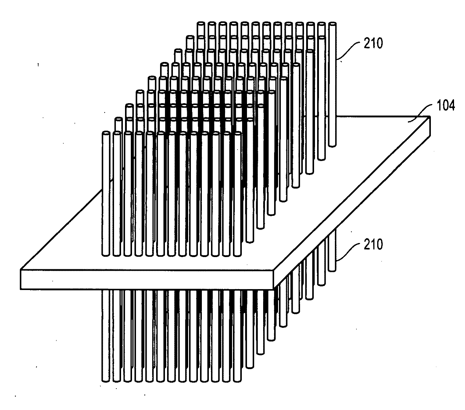
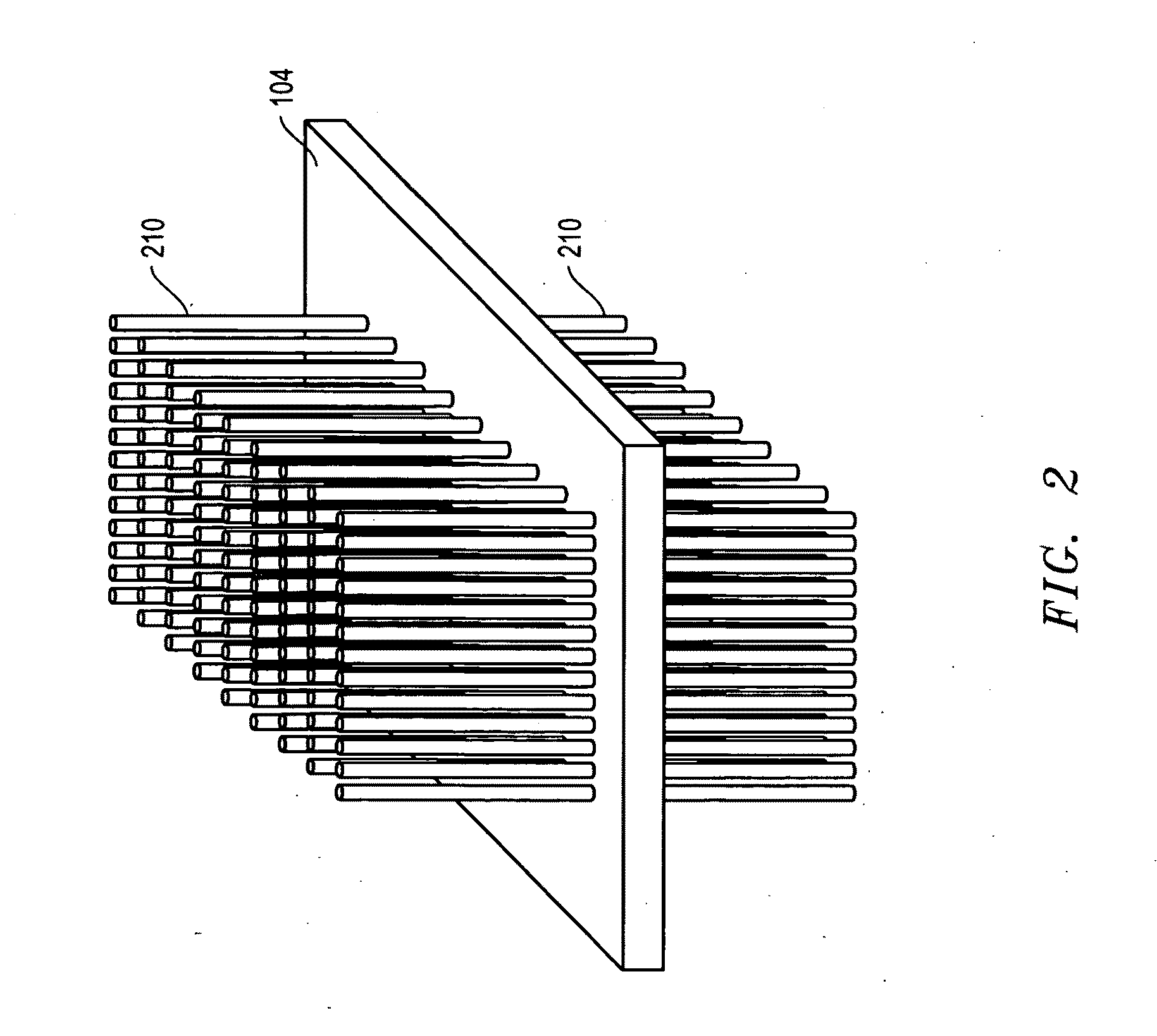
[0010]In one embodiment, relatively short CNT forests (e.g. from about 0.1 mm to about 0.5 mm in length) may be grown in a solderless manner on both sides of the contacts in a captured contact array. The captured contact array may be sandwiched between devices with fixed contacts (PCB, IC
package, bare die, flip-
chip die) and a
target surface with fixed contacts (such as a PCB, IC package, bare die, or
hybrid substrate) end then mechanically constrained with a
retainer clip. The
retainer clip may then be removed so that the component may be easily lifted off the board. Even with very fine component contact pitches (e.g., such has 0.050 inch), CNT
fiber sizes still provide thousands of contact points in this embodiment. Moreover, the flexibility of the CNT forest acts to account for and compensate for irregularities in rigid part contact geometries as well as any mismatch in the CTE between the two rigid surfaces.
[0011]In another embodiment, relatively short CNT forests (e.g., from about 0.1 mm to about 0.5 mm in length) may be grown in a solderless manner directly on the contacts of a rigid surface such as a PCB, IC package, or bare die. When this rigid surface is then mechanically constrained to a
target surface with matching fixed contacts (such as a PCB, IC package, bare die, or hybrid substrate), reliable electrical contact is established. When the constraint is then removed, the surfaces may easily be separated. For example, in one exemplary implementation, multiple die may be assembled in a stack one upon another and then mechanically constrained with a
retainer clip in order to facilitate electrical contact and
interconnection between the individual devices. When the retainer clip is then removed, the various die of the stacked
assembly may be easily separated, e.g., to accommodate for repair and / or
upgrade activities, and / or eliminating the yield and manufacturing losses related to “known good die” issues. Even with the finest die contact pitches (e.g., such as 0.010″), CNT
fiber sizes still allow for thousands of contact points in this embodiment. Moreover, the flexibility of the CNT forest acts to account for irregularities in rigid die contact geometries (steps, plateaus, and other shapes) as well as mismatch in the CTE between various die. The
thermal conductivity of the CNT fibers also allows for heat conduction through the die stack.
[0012]In yet another embodiment, relatively short CNT forests (e.g., from about 0.1 mm to about 0.5 mm in length) may be grown in a solderless manner and in a pattern on the contacts of an
integrated circuit package known as a “flip-chip”. Such packages ordinarily include a die which is soldered in place in the package using BGA-style “bump” contacts on one side of the die. However, in one embodiment of the disclosed apparatus and methods, a
flip chip type die with fixed contacts may be placed on the CNT contact array in the package and then mechanically constrained in order for the part to make contact with the package. In such an embodiment, when the package is opened, the die may be easily removed and replaced. Even the finest die contact pitches (0.010″), CNT fiber sizes still allow for thousands of contact points in this embodiment. Moreover, the flexibility of the CNT forest accounts for irregularities in rigid die contact geometries as well as mismatch in the CTE between the component and package materials.
[0013]In yet another embodiment, one or more relatively short CNT forests (e.g., from about 0.1 mm to about 0.5 mm in length) may be grown in a solderless manner directly on an
edge connector contact pad of a rigid surface such as a PCB. When this
edge connector contact pad is then inserted between
mating spring contacts of a card
edge connector, reliable electrical contact is established. Alternatively, one or more relatively short CNT forests may be grown on contact surfaces of card edge connector spring contacts to achieve reliable electrical contact with a edge connector pad of a PCB or other card.
[0014]In yet another embodiment, one or more relatively short CNT forests (e.g., from about 0.1 mm to about 0.5 mm in length) may be grown in a solderless manner directly on a rigid contact surface of a
connector pin. When this
connector pin is then inserted between
mating spring contacts of a socket connector, reliable electrical contact is established. Alternatively, one or more relatively short CNT forests may be grown on contact surfaces of a socket connector spring contact to achieve reliable electrical contact with a
connector pin.

