Methods and structures for highly efficient hot carrier injection programming for non-volatile memories

a non-volatile memory, high-efficiency technology, applied in the direction of digital storage, instruments, semiconductor devices, etc., can solve the problems of low programming efficiency, difficult charge pump circuit design, and inability to meet the requirements of the charge pump, so as to improve the programming efficiency, and reduce the current of the devi

a non-volatile memory, high-efficiency technology, applied in the direction of digital storage, instruments, semiconductor devices, etc., can solve the problems of low programming efficiency, difficult charge pump circuit design, and inability to meet the requirements of the charge pump, so as to improve the programming efficiency, and reduce the current of the devi

US20090021984A1Active Publication Date: 2009-01-22PEGASUS SEMICON SHANGHAI CO LTD

Image

  • Methods and structures for highly efficient hot carrier injection programming for non-volatile memories
  • Methods and structures for highly efficient hot carrier injection programming for non-volatile memories
  • Methods and structures for highly efficient hot carrier injection programming for non-volatile memories

Examples


Embodiment Construction

[0016]The present invention includes methods and structures to optimize the Hot Carrier Injection programming for NVM cells. Those of ordinary skill in the art will immediately realize that the embodiments of the present invention described herein are illustrative only and are not intended to be in any way limiting. Other embodiments of the present invention will readily suggest themselves to such skilled persons having the benefits of this disclosure.

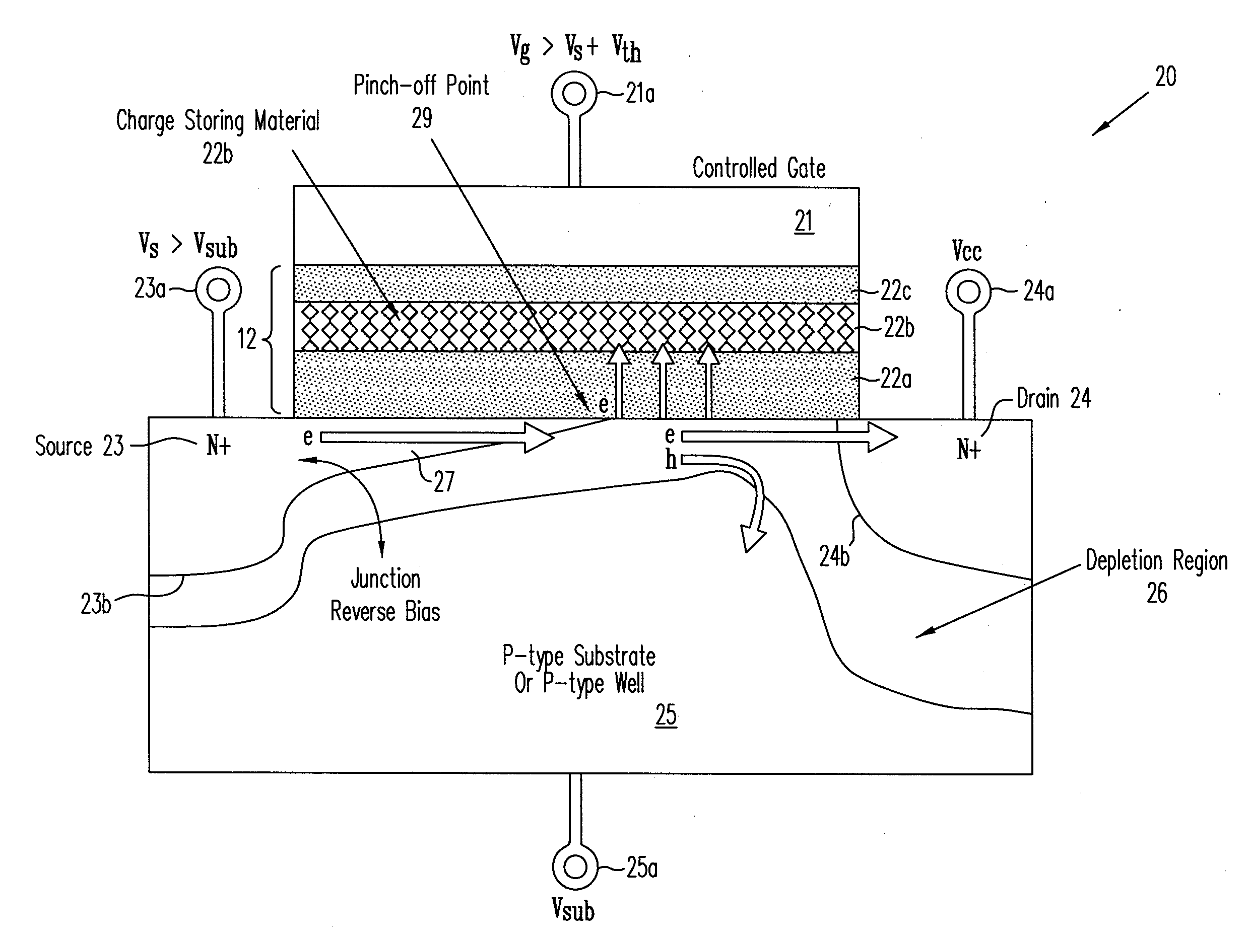
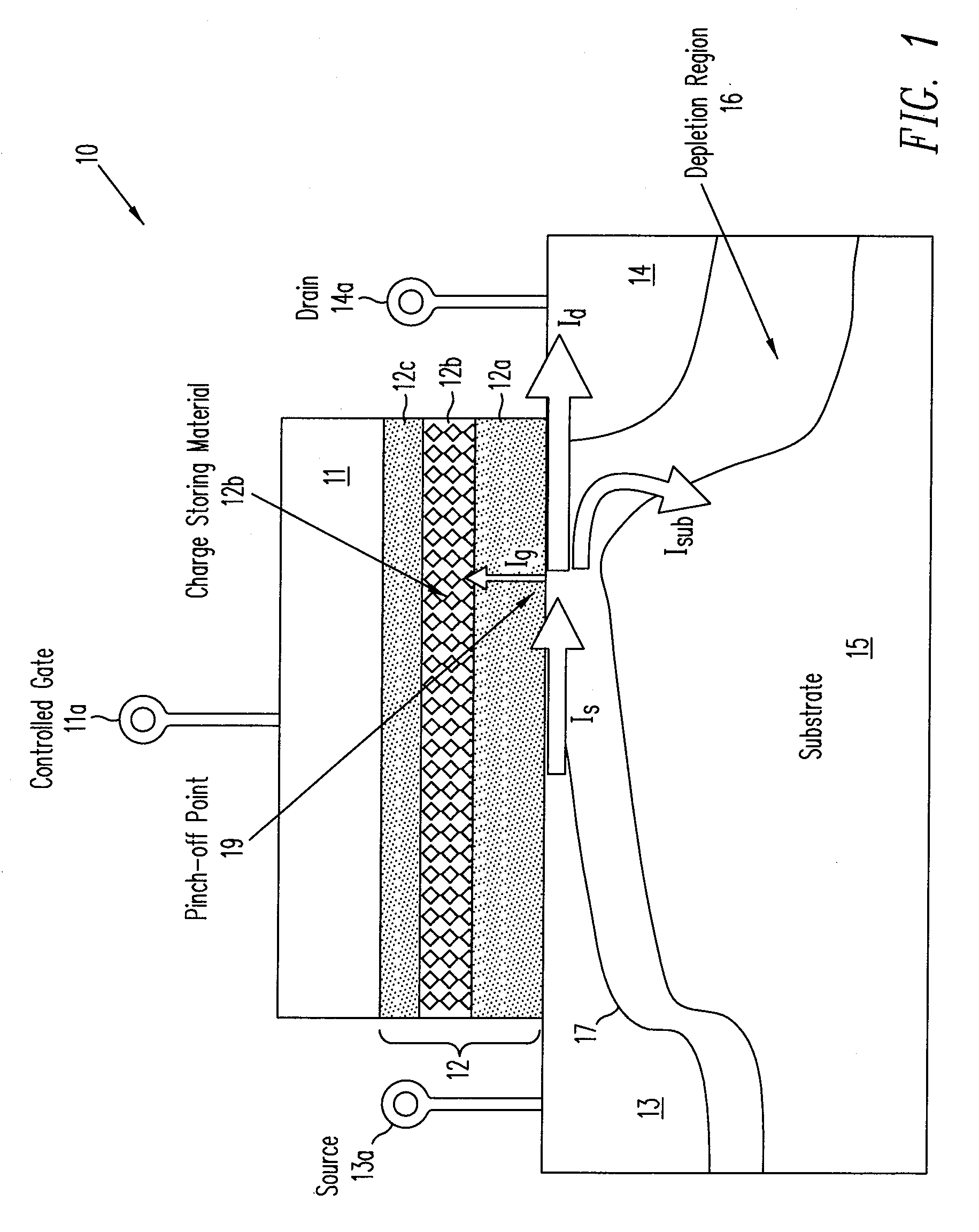
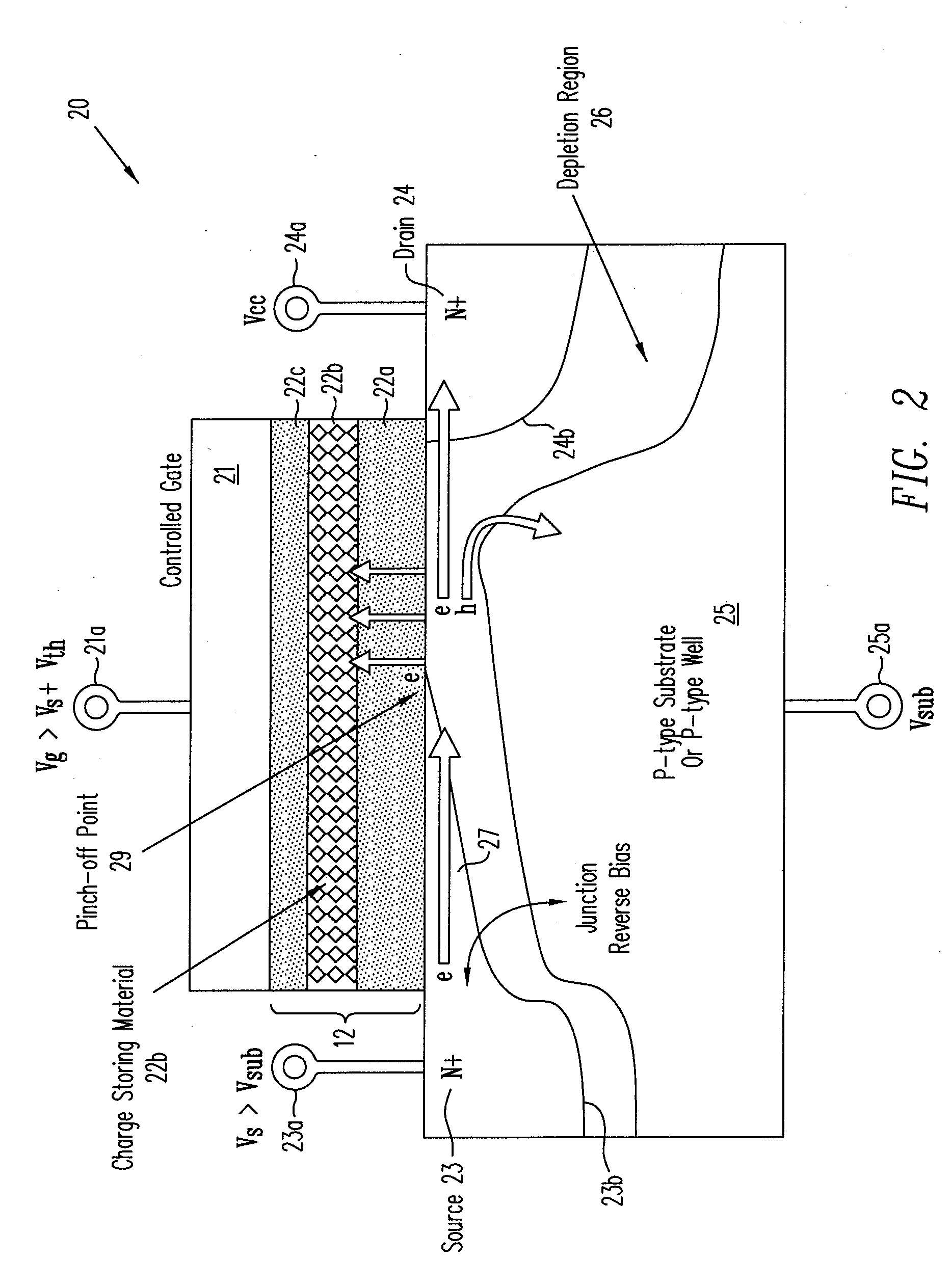
[0017]In one aspect of this invention, an N-type Non-Volatile Memory (NVM) device 20 as shown in FIG. 2 includes N-type source 23 and drain 24 regions in a P-type substrate 25. The control gate 21 is on top of but separated from the substrate 25 by thin dielectrics 22a and 22c and storing material 22b embedded in the thin dielectric 12. By applying a positive voltage to control gate 21, an N-type channel region is formed between source 23 and drain 24 in the top surface of substrate 25. During the HCI programming, the drain electrode 2...


PUM


Abstract

A metal oxide semiconductor field effect transistor (MOSFET) in a non-volatile memory cell has a source, a drain and a channel region between the source and the drain, all formed in a substrate of opposite conductivity type to the conductivity type of the source and drain. The MOSFET is programmed by connecting the drain electrode to the supply source of the main voltage, Vcc, provided to said non-volatile memory cell and supplying selected voltages to the source and substrate so as to invert a portion of the channel region extending from the source toward the drain. The inverted portion of the channel region ends at a pinch-off point before reaching the drain. By controlling the reverse bias across the PN junction between the source and the substrate, the pinch-off point of the inversion region is pulled back toward the source thereby to increase the programming efficiency of the MOSFET.Methods and structures for highly efficient Hot Carrier Injection (HCI) programming for Non-Volatile Memories (NVM) apply the main positive supply voltage Vcc to, the drain electrode of the NVM cell from the chip main voltage supply in contrast to the conventional method using a higher voltage than Vcc. The source electrode and substrate are reverse biased with a differential voltage relative to the drain, while a voltage pulse is applied to the control gate of the NVM cell to turn on the NVM cell for programming. To optimize the programming condition, the source voltage and the substrate voltage are then adjusted to achieve the maximum threshold voltage shifts under the same applied gate voltage pulse condition (i.e. using a gate pulse with the same voltage amplitude and duration regardless of the source voltage and the substrate voltage). The substrate voltage to the drain voltage can not exceed the avalanche multiplication junction breakdown for a small programming current during the bias voltage adjustment.

Description

FIELD OF INVENTION[0001]This invention relates to methods and structures for programming Non-Volatile Memory (NVM) cells using highly efficient Hot Carrier Injection (HCI).BACKGROUND OF INVENTION[0002]As shown in FIG. 1, metal oxide semiconductor field effect transistor 10 (MOSFET) includes a source 13 and a drain 14 (connected respectively to source electrode 13a and drain electrode 14a) each with an impurity type opposite to the impurity type of the substrate 15. The source 13 and drain 14 are separated by a channel region in the substrate 15 underlying a control gate 11 formed over a dielectric layer 12 on top of the silicon substrate 15. When the voltage applied to the gate electrode 11a electrically connected to control gate 11 exceeds the threshold voltage of the MOSFET 10, the channel region in the substrate 15 between the source 13 and the drain 14 and just below the dielectric 12 under the control gate 11 of the MOSFET device 10 is inverted to the same conductivity type as ...

Claims


Application Information

Patent Timeline
22 Jan 2009
Publication
US20090021984A1
IPC
G11C11/34
CPC
G11C8/08; G11C2216/10; G11C16/10; H01L29/7883
Inventors
WANG, LEE