IrOx Nanostructure Electrode Neural Interface Optical Device

a neural interface and nanostructure technology, applied in the field of integrated circuit (ic) fabrication, can solve the problems of limited charge an electrode can deliver, easy damage to the retina, and high resistance of tissue to electrical stimulation

Active Publication Date: 2009-01-22
SHARP KK
View PDF12 Cites 27 Cited by
  • Summary
  • Abstract
  • Description
  • Claims
  • Application Information

AI Technical Summary

Problems solved by technology

One major difficulty with the epiretinal approach is that the tissue has a very high resistance to electrical stimulation.
The power output needs to be strictly controlled, since heat dissipation is limited in the subretinal space, and overheating can easily damage the retina.
One technical challenge is the trade-off between electrode density and stimulation charge.
Although the total charge injection required to elicit a visual percept is fixed, the maximum charge an electrode can deliver is limited by its surface area.
Surpassing this charge density threshold generates undesirable and irreversible electrochemical reactions.
However, a key issue to be resolved is the fabrication of an electrode array that can conform to the concave shape of the foveal pit.
Another limitation associated with micromachining technology is size, as the individually machined electrodes cannot be made to a nano-size resolution.
Even if a template of nano-sized structures could be micro-machined, plating an array of nanostructures, with a noble metal for example, in a sufficiently high aspect ratio is a big challenge.
However, it is difficult to form single-crystal IrO2 films using conventional PVD or electrode plating methods.
IrO2 nanostructures can be formed using a solution method, but these structures have a low mechanical strength and poor crystal quality.
Vapor phase transport methods can also be used to form IrO2nanostructures, but this process requires high substrate temperature, and it is not suitable for use with glass and polyimide substrates.

Method used


Image

  • IrOx Nanostructure Electrode Neural Interface Optical Device
  • IrOx Nanostructure Electrode Neural Interface Optical Device
  • IrOx Nanostructure Electrode Neural Interface Optical Device

Examples


Embodiment Construction

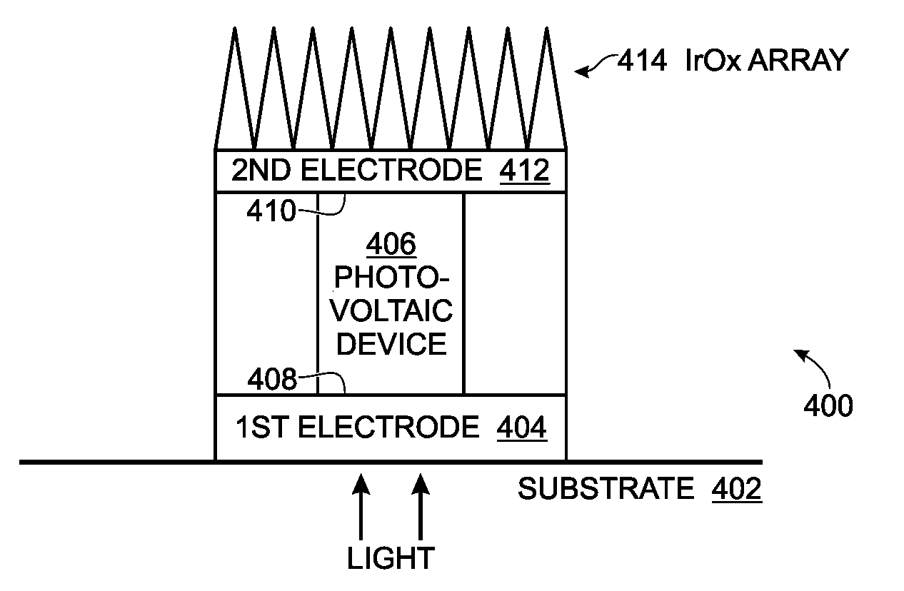
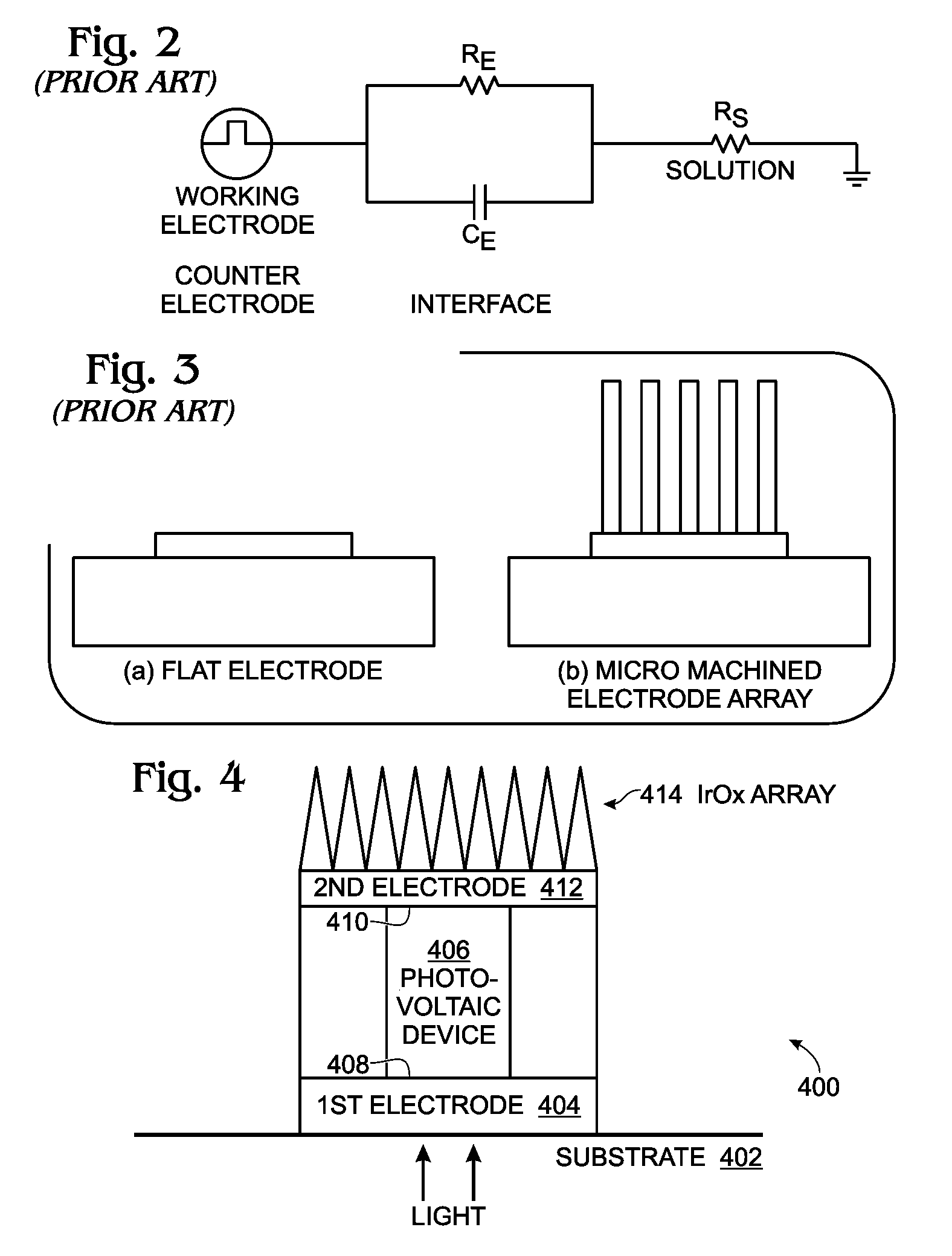
[0038]FIG. 4 is a partial cross-sectional view of an optical device with an iridium oxide (IrOx) electrode neural interface. The device 400 comprises a substrate 402 and a first conductive electrode 404 overlying the substrate 402. The substrate 402 can be a material such as glass, quartz, plastic, or a flexible polyimide. However, the device 400 is not limited to just these exemplary materials.

[0039]A photovoltaic device 406 has a first electrical interface 408 connected to the first electrode 404, and a second electrical interface 410. A second conductive electrode 412 overlies the photovoltaic device 406 and is connected to the second electrical interface 410. An array of neural interface single-crystal IrOx (x≦4) nanostructures 414 overlies the second electrode 412. As used herein, a nanostructure is a structure having nano-sized feature, as defined in more detail below, which may also be referred to as nanowires, nanotubes, nanorods, or the like. Due to the fabrication methods,...


PUM


Abstract

An optical device with an iridium oxide (IrOx) electrode neural interface, and a corresponding fabrication method are provided. The method provides a substrate and forms a first conductive electrode overlying the substrate. A photovoltaic device having a first electrical interface is connected to the first electrode. A second electrical interface of the photovoltaic device is connected to a second conductive electrode formed overlying the photovoltaic device. An array of neural interface single-crystal IrOx nanostructures are formed overlying the second electrode, where x≦4. The IrOx nanostructures can be partially coated with an electrical insulator, such as SiO2, SiN, TiO2, or spin on glass (SOG), leaving the IrOx distal ends exposed. In one aspect, a buffer layer is formed overlying the second electrode surface, made from a material such as LiNbO3, LiTaO3, or SA, for the purpose of orienting the growth direction of the IrOx nanostructures.

Description

RELATED APPLICATIONS[0001]This application is a Divisional of a pending application entitled, OPTICAL DEVICE WITH IrOx NANOSTRUCTURE ELECTRODE NEURAL INTERFACE, invented by Zhang et al, Ser. No. 11 / 496,157, filed Jul. 31, 2006, Attorney Docket No. SLA8084;[0002]which is a continuation-in-part of an application entitled, IRIDIUM OXIDE NANOTUBES AND METHOD FOR FORMING SAME, invented by Zhang et al., Ser. No. 10 / 971,280, filed Oct. 21, 2004, now U.S. Pat. No. 7,008,144.[0003]The Ser. No. 11 / 496,157 application is also a continuation-in-part of an application entitled, IRIDIUM OXIDE NANOWIRE AND METHOD FOR FORMING SAME, invented by Zhang et al., Ser. No. 10 / 971,330, filed Oct. 21, 2004, now U.S. Pat. No. 7,255,745.[0004]All of the above-mentioned applications are incorporated herein by reference.BACKGROUND OF THE INVENTION[0005]1. Field of the Invention[0006]This invention generally relates to integrated circuit (IC) fabrication and, more particularly, to an optical device with an iridi...

Claims


Application Information

Patent Timeline
Patent Type & Authority Applications(United States)
IPC IPC(8): A61N1/36
CPCA61N1/0543B82Y5/00B82Y10/00C30B29/605C30B25/00C30B29/16B82Y30/00Y10S977/811Y10S977/904Y10S977/932
Inventor ZHANG, FENGYANHSU, SHENG TENG
Owner SHARP KK
Why Eureka
Try Eureka