

Method and materials for patterning a neutral surface
a neutral surface and material technology, applied in the direction of photosensitive materials, instruments, photomechanical equipment, etc., can solve the problems of increasing the probability of unwanted signal propagation, process suffers from additional complexity, and the product of rc in the chip is reduced, so as to enhance the properties of the diblock copolymer
- Summary
- Abstract
- Description
- Claims
- Application Information
AI Technical Summary
Benefits of technology
Problems solved by technology
Method used
Image

Examples
Embodiment Construction
Field of the Invention
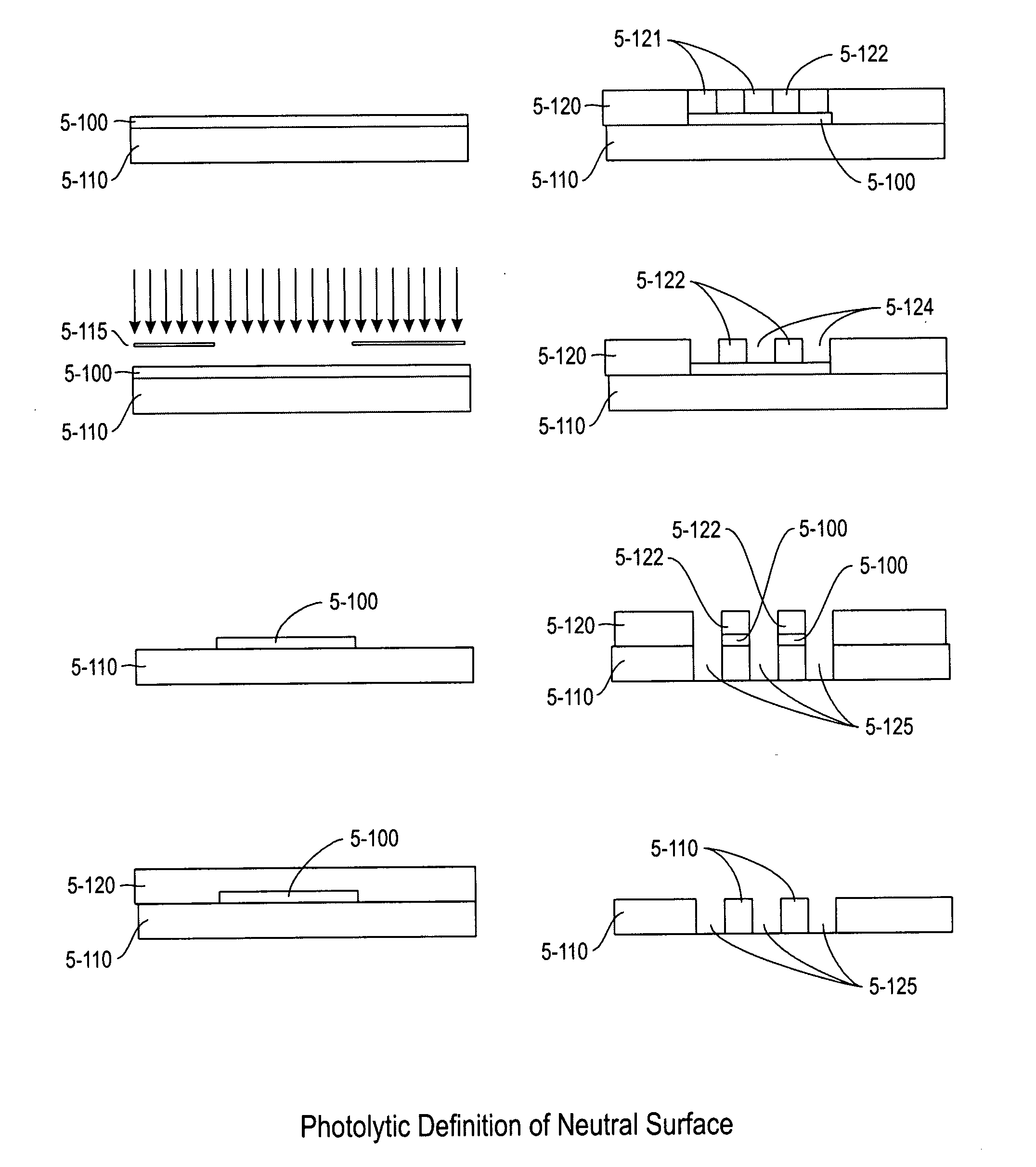
[0001]The field of the invention comprises convolved self-assembled structures such as nanostructures, and the fabrication of such structures by processes such as deterministic patterning processing methods, e.g., deterministic photolithography, which comprises the use of a master, such as a photolithographic mask to direct self-assembly in a predetermined location. Ion beam etching and other etch techniques known in the art can also be employed.
[0002]More specifically, and in one aspect, the fabrication comprises the generation of nanostructures by photolithography to pre-define regions in the structure where self assembly takes place.
BACKGROUND OF THE INVENTION
[0003]The advancement of semiconductor computational speed has largely been driven by the ever smaller dimensions of semiconductor transistors and other integrated circuit (IC) components brought about by scaling their dimensions and / or properties.
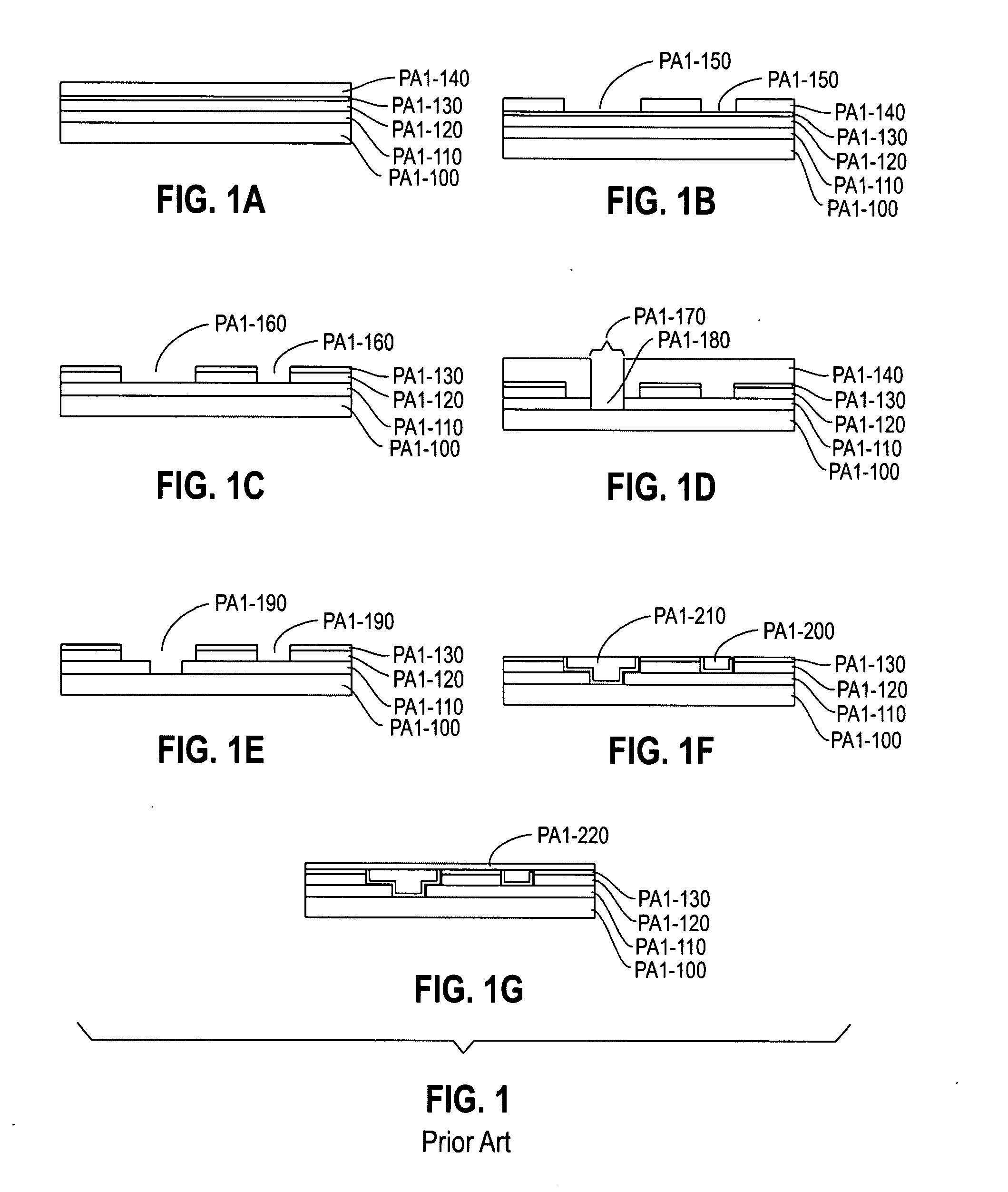
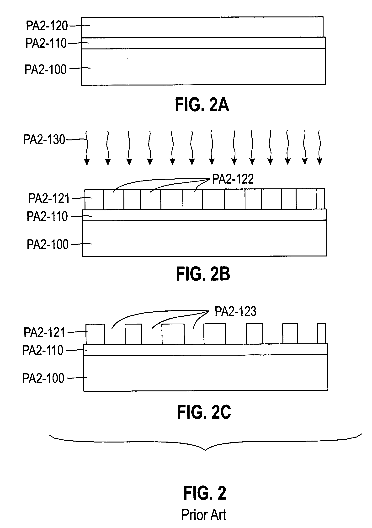
[0004]Most of these processes rely on separate patternin...
PUM
 Abstract
Description
Claims
Application Information