Display device and manufacturing method thereof
a technology of a display device and a manufacturing method, which is applied in the direction of semiconductor devices, basic electric elements, electrical appliances, etc., can solve the problems of easy oxidation of the surface of a microcrystalline semiconductor film, and the electric characteristics of a thin film transistor are decreased, so as to improve the reliability of a transistor and a display device having a transistor, the effect of improving the electrical characteristics of a transistor and a transistor
- Summary
- Abstract
- Description
- Claims
- Application Information
AI Technical Summary
Benefits of technology
Problems solved by technology
Method used
Image

Examples
embodiment mode 1
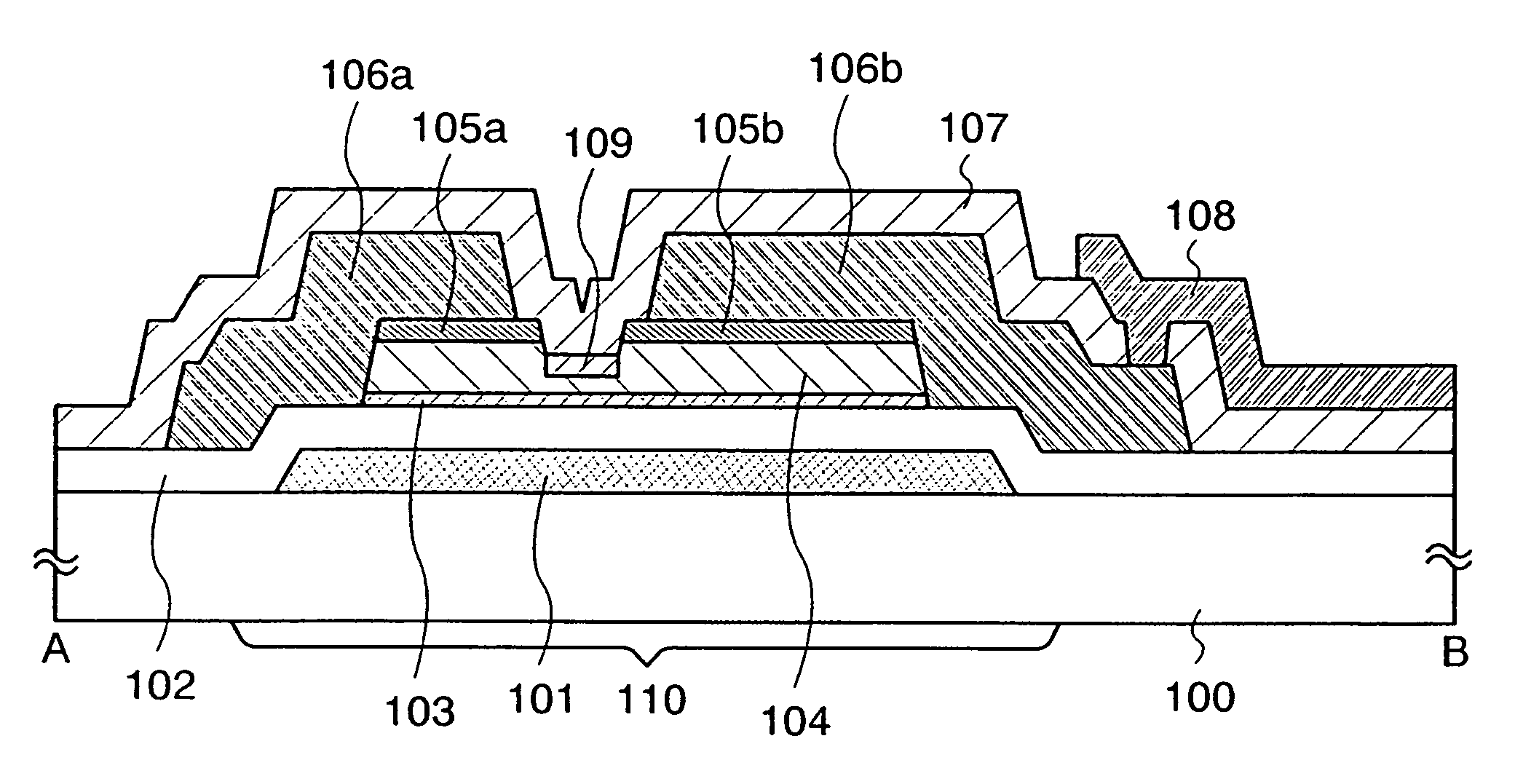
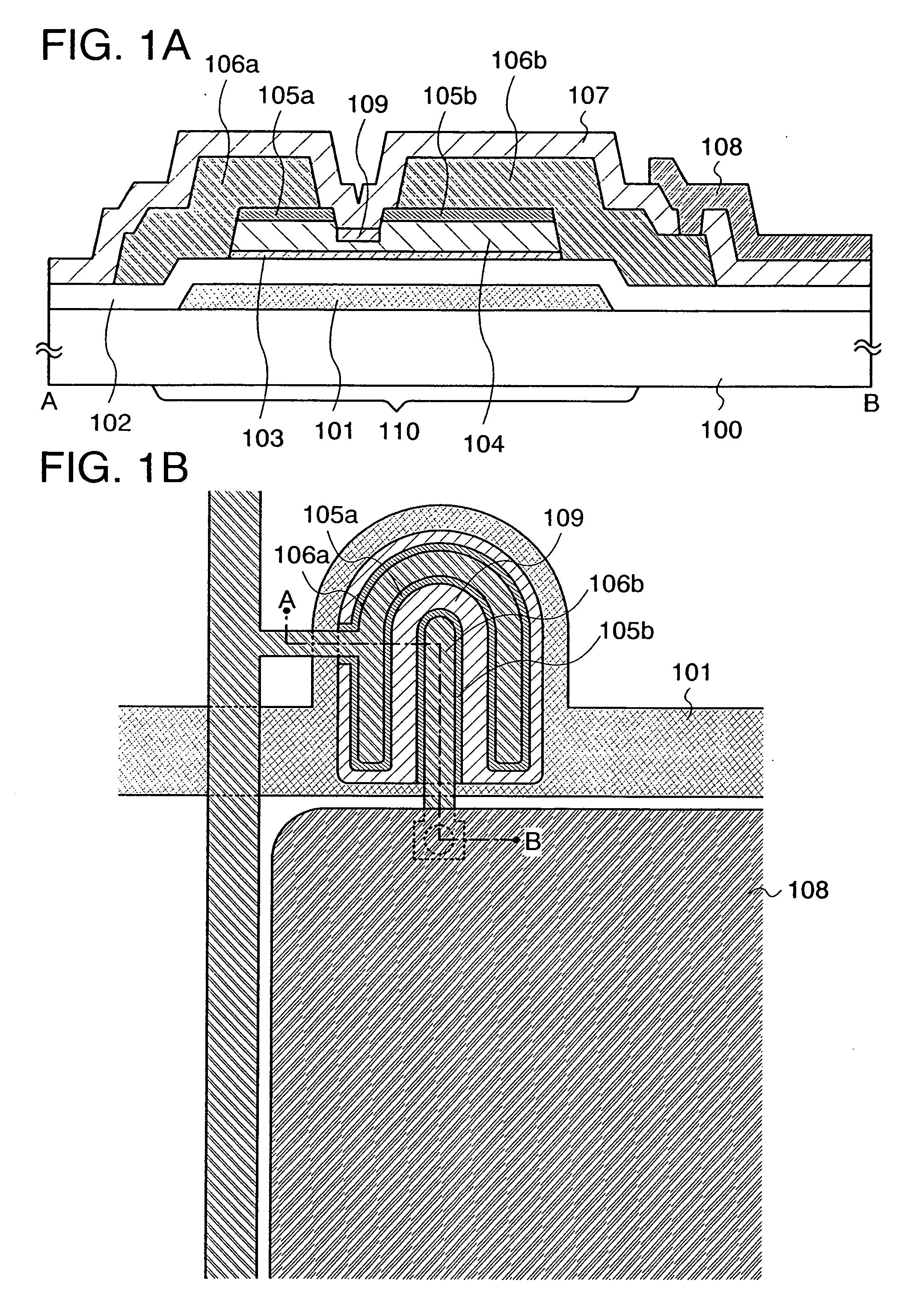
[0046]In this embodiment mode, a bottom-gate thin film transistor (TFT) used for a display device is described with reference to drawings. FIGS. 1A and 1B are a cross-sectional view and a top view of a thin film transistor and a pixel electrode electrically connected to the thin film transistor in part of a pixel, respectively. FIG. 1A corresponds to a cross section taken along the line A-B in FIG. 1B.
[0047]A thin film transistor 110 included in a display device includes a gate electrode 101 provided over a substrate 100, a first semiconductor layer 103 which is provided over the gate electrode 101 through a gate insulating film 102 and has a microcrystalline semiconductor, a second semiconductor layer 104 which is provided over the first semiconductor layer 103 and has an amorphous semiconductor, an impurity region 109 provided in part of the second semiconductor layer 104, a source region 105a and a drain region 105b which are provided over the second semiconductor layer 104, and ...
embodiment mode 2
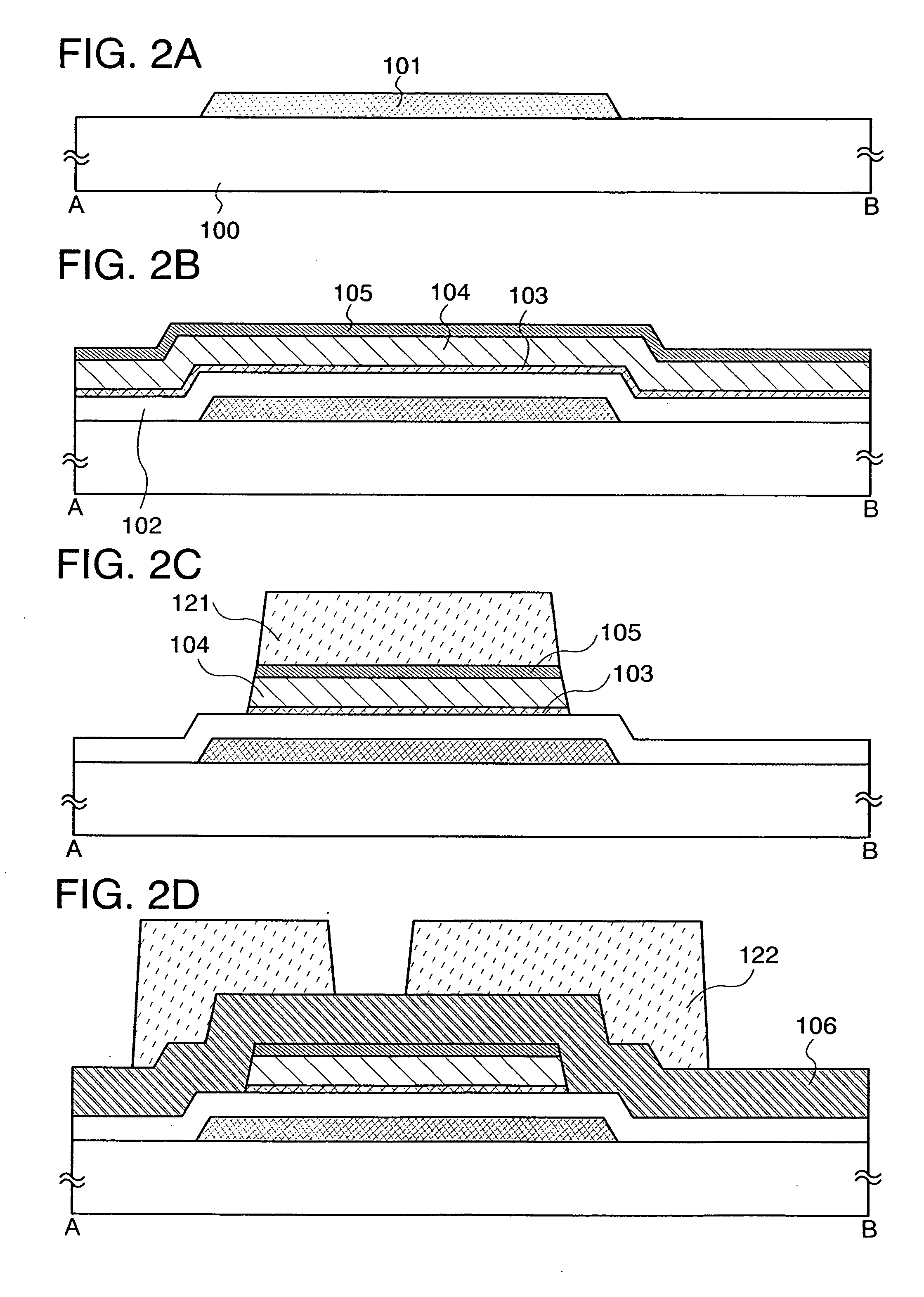
[0065]In this embodiment mode, a method for manufacturing the bottom-gate thin film transistor used for a display device, which is described in Embodiment Mode 1, is described with reference to drawings. An n-channel thin film transistor is described below.
[0066]First, the gate electrode 101 is formed over the substrate 100 (see FIG. 2A and FIG. 5A).
[0067]As the substrate 100, any of the following substrates can be used: an alkali-free glass substrate formed of barium borosilicate glass, aluminoborosilicate glass, aluminosilicate glass, or the like by a fusion method or a float method; a ceramic substrate; a plastic substrate having heat resistance enough to withstand a process temperature of this manufacturing process; and the like. Alternatively, a metal substrate of a stainless alloy or the like with the surface provided with an insulating layer may be used. When the substrate 100 is a mother glass, the substrate may have any of the following sizes: the first generation (e.g., 32...
embodiment mode 3
[0156]In this embodiment mode, a display device including a thin film transistor which is different from the thin film transistors in the aforementioned embodiment modes is described with reference to FIG. 18.
[0157]Comparing the structure shown in FIGS. 1A and 1B, the thin film transistor 110 shown in this embodiment mode includes a semiconductor layer 140a containing an impurity element at a low concentration, which is provided between the second semiconductor layer 104 and the source region 105a, and a semiconductor layer 140b containing an impurity element at a low concentration, which is provided between the second semiconductor layer 104 and the drain region 105b (see FIG. 18). When the semiconductor layers 140a and 140b are provided, electric field concentration between the second semiconductor layer 104 and the source region 105a or between the second semiconductor layer 104 and the drain region 105b can be relieved.
[0158]In FIG. 18, when the thin film transistor is an n-chan...
PUM
 Abstract
Description
Claims
Application Information