Method of depositing silicon oxide films

a silicon oxide film and film technology, applied in the field of thin film deposition, can solve the problems of deviating the refractive index (ri), inconsistent etch selectivity, and silicon oxide films deposited by high-temperature cvd processes such as lpcvd or apcvd,

Inactive Publication Date: 2009-02-12
ASM KOREA LTD
View PDF22 Cites 436 Cited by
  • Summary
  • Abstract
  • Description
  • Claims
  • Application Information

AI Technical Summary

Problems solved by technology

Silicon oxide films deposited by a high temperature CVD process, such as LPCVD or APCVD, tend to have defects, such as interface oxidation and dopant diffusion.
Such defects may degrade electrical characteristics of devices that include the silicon oxide films.
Such hydrogen and nitrogen atoms in the films may adversely affect the processing of the films, and result in a deviated refractive index (RI) and inconsistent etch selectivity.

Method used


Image

  • Method of depositing silicon oxide films
  • Method of depositing silicon oxide films
  • Method of depositing silicon oxide films

Examples


first embodiment

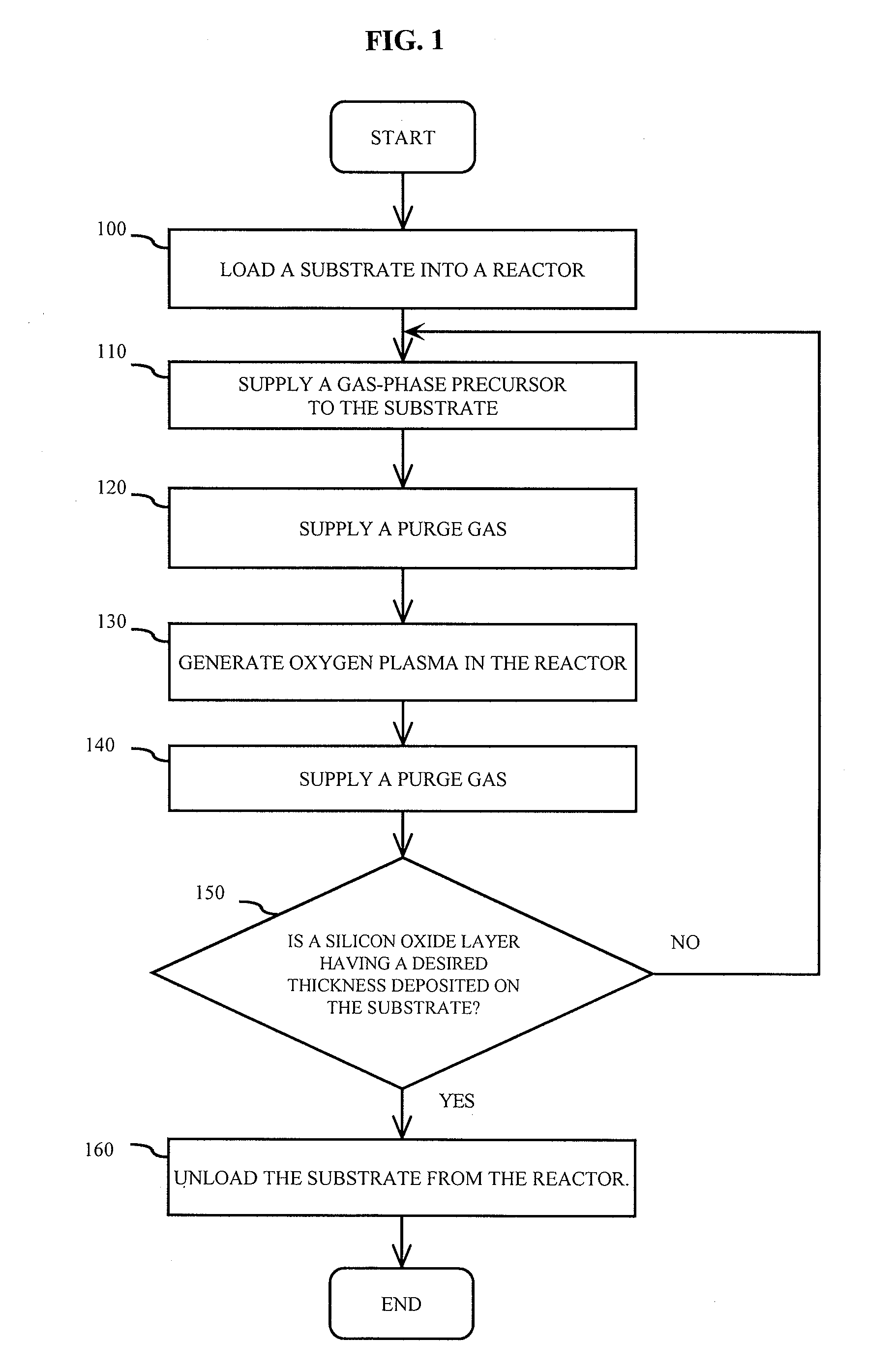
[0021]A method of depositing a silicon oxide film will be described with reference to FIG. 1. FIG. 1 is a flowchart illustrating a cyclical method of depositing a silicon oxide film.

[0022]First, a substrate on which a silicon oxide film is to be deposited is loaded into a reactor (step 100). In one embodiment, the substrate may be a wafer formed of silicon. In other embodiments, the substrate may be formed of any other suitable material. The substrate may include one or more layers or features (for example, lines, islands, trenches, etc.) formed thereon.

[0023]In one embodiment, the reactor may be a chemical vapor deposition (CVD) reactor. In another embodiment, the reactor may be an atomic layer deposition (ALD) reactor. Examples of reactors include, but are not limited to, those described in U.S. Pat. No. 6,539,891; U.S. Pat. No. 6,645,574; U.S. Patent Application Publication No. 2005 / 0034664; U.S. Patent Application Publication No. 2006 / 0249077; and U.S. Patent Application Public...

second embodiment

[0038]Referring to FIG. 4, a method of depositing a silicon oxide film will be described below. FIG. 4 illustrates gas supply cycles for the method.

[0039]In the illustrated method, a substrate on which a silicon oxide film is to be deposited is loaded into a reactor. The details of the substrate can be as described above with respect to the substrate of FIG. 1. In one embodiment, the reactor may be a chemical vapor deposition (CVD) reactor. In another embodiment, the reactor may be an atomic layer deposition (ALD) reactor. Examples of reactors include, but are not limited to, those described in U.S. patent application Ser. No. 12 / 058,364, filed on Mar. 28, 2008, entitled LATERAL FLOW DEPOSITION APPARATUS AND METHOD OF DEPOSITING FILM BY USING THE APPARATUS, the disclosure of which is incorporated herein by reference in its entirety for purposes of describing a suitable reactor for implementing the second embodiment.

[0040]Then, a reactant gas R, such as ozone (O3), is substantially ...


PUM

PropertyMeasurementUnit
temperatureaaaaaaaaaa
pressureaaaaaaaaaa
pressureaaaaaaaaaa

Abstract

Methods of depositing a silicon oxide film are disclosed. One embodiment is a plasma enhanced atomic layer deposition (PEALD) process that includes supplying a vapor phase silicon precursor, such as a diaminosilane compound, to a substrate, and supplying oxygen plasma to the substrate. Another embodiment is a pulsed hybrid method between atomic layer deposition (ALD) and chemical vapor deposition (CVD). In the other embodiment, a vapor phase silicon precursor, such as a diaminosilane compound, is supplied to a substrate while ozone gas is continuously or discontinuously supplied to the substrate.

Description

CROSS-REFERENCE TO RELATED APPLICATIONS[0001]This application claims priority under 35 U.S.C. §119(a) to and the benefit of Korean Patent Application No. 10-2007-0080581 filed in the Korean Intellectual Property Office on Aug. 10, 2007, the entire disclosure of which is incorporated herein by reference.BACKGROUND OF THE INVENTION[0002]1. Field of the Invention[0003]The present invention relates to deposition of thin films. More particularly, the present invention relates to a method of depositing silicon oxide films.[0004]2. Description of the Related Art[0005]In depositing silicon oxide films for semiconductor devices, chemical vapor deposition (CVD) methods, such as low pressure CVD (LPCVD), atmospheric pressure CVD (APCVD), and plasma-enhanced CVD (PECVD), have been widely used. In LPCVD or APCVD, two or more source gases can be simultaneously supplied and deposited at a relatively high temperature (for example, about 500° C. to about 850° C.) to form a silicon oxide film over a ...

Claims


Application Information

Patent Timeline
Patent Type & Authority Applications(United States)
IPC IPC(8): H05H1/24
CPCC23C16/45542C23C16/402H01L21/205H01L21/76229H01L23/535H01L23/647C04B35/14Y10T428/31504C01B33/113C23C16/401C23C16/4408H01L21/02164H01L21/02274
Inventor YOON, TAE HOPARK, HYUNG SANGYOO, YONG MIN
Owner ASM KOREA LTD
Why Eureka
Try Eureka