Electronic device with a layer structure of organic layers

Active Publication Date: 2009-02-19
NOVALED AG
View PDF99 Cites 121 Cited by
  • Summary
  • Abstract
  • Description
  • Claims
  • Application Information

AI Technical Summary

Benefits of technology

[0027]The inventors surprisingly found that long operation lifetimes of organic semiconductor devices comprising a p-n-junction in a structure of organic layers can be achieved by using molecular dopants for the p- and n-type doped layers at the p-n-interface which allows for a tailoring of the interface stability. With the use of m

Problems solved by technology

They also might reduce the injection barrier from the transport layers into the emission zone, therefore leading to reduced operating voltages of the electroluminescent device.
They feature extremely low operating voltages, often being close to the thermodynamical limit set by the wavelength of the emitted light.
Within a production process, these additional layers will cause additional costs, especially as these layers might be produced with different types of evaporation sources than the other organic layers within the stacked OLED devices.
However, the approach demonstrated still requires the introduction of layers in addition to the layers used within the OLED units.
A significant drawback of the approach is the fact, that the organic layers forming the p-n-junction are doped

Method used


Image

  • Electronic device with a layer structure of organic layers
  • Electronic device with a layer structure of organic layers
  • Electronic device with a layer structure of organic layers

Examples


example 1

Conventional

[0098]According to Example 1a structure for a conventional light emitting device is provided as follows:[0099]1.1 50 nm 2,2′,7,7′-Tetrakis-(N,N-di-methylphenylamino)-9,9′-spirobifluorene doped with 2-(6-Dicyanomethylene-1,3,4,5,7,8-hexafluoro-6H-naphtalen-2-ylidene)-malononitrile (p-type doped hole-transport layer);[0100]1.2 10 nm NPB (interlayer);[0101]1.3 20 nm Spiro-DPVBI;[0102]1.4 10 nm Bphen;[0103]1.5 45 nm Bphen doped with Cs (n-type doped electron-transport layer);[0104]1.6 50 nm 2,2′,7,7′-Tetrakis-(N,N-di-methylphenylamino)-9,9′-spirobifluorene doped with 2-(6-Dicyanomethylene-1,3,4,5,7,8-hexafluoro-6H-naphtalen-2-ylidene)-malononitrile (p-type doped hole-transport layer);[0105]1.7 10 nm NPB (interlayer);[0106]1.8 20 nm Spiro-DPVBI;[0107]1.9 10 nm Bphen;[0108]1.10 20 nm Bphen doped with Cs (n-type doped electron-transport layer);[0109]1.11 100 nm Aluminum (reflective cathode).

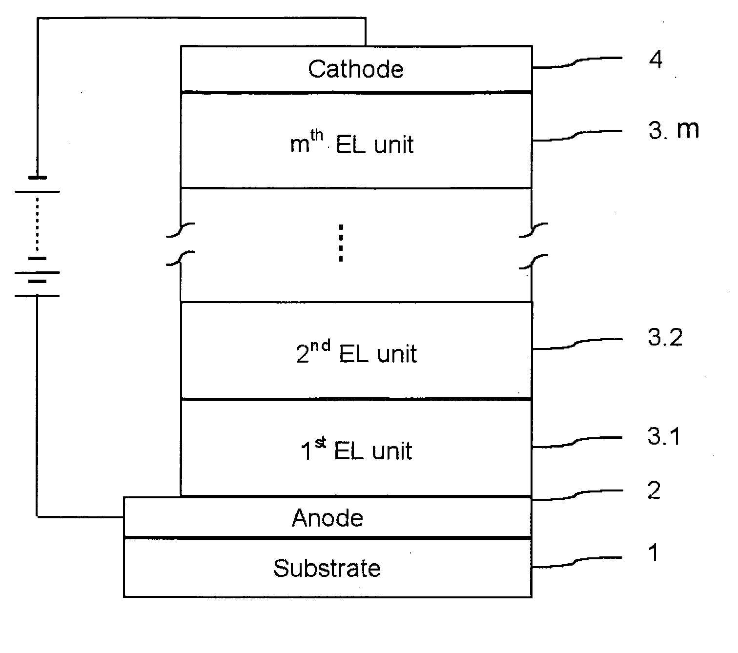
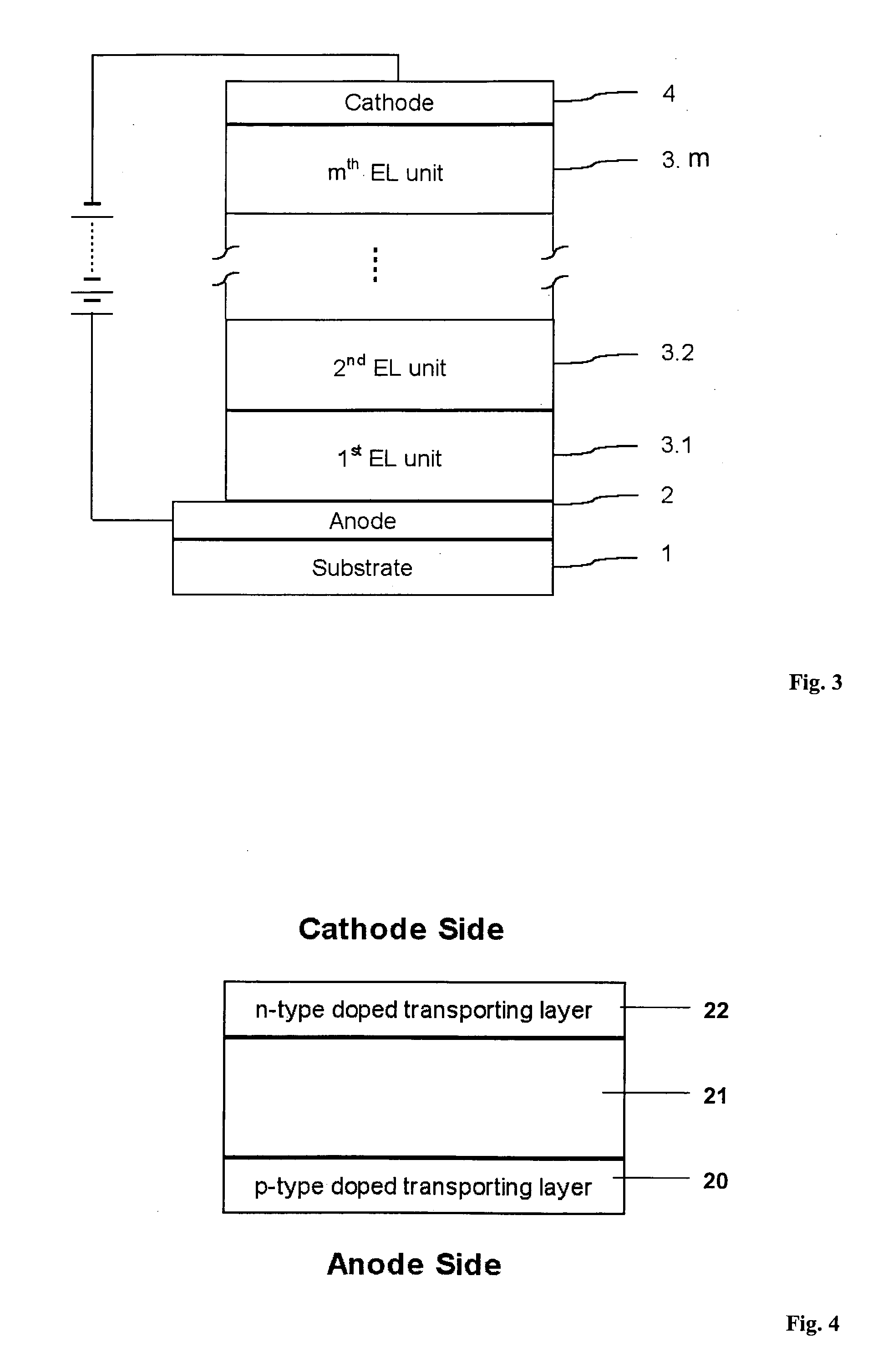
[0110]This is a blue stacked PIN-OLED where layers 1.1 to 1.5 constitute a first PIN-OLE...

example 2

[0113]According to Example 2a structure for a light emitting device is provided as follows:[0114]2.1 50 nm 2,2′,7,7′-Tetrakis-(N,N-di-methylphenylamino)-9,9′-spirobifluorene doped with 4 mole % 2-(6-Dicyanomethylene-1,3,4,5,7,8-hexafluoro-6H-naphtalen-2-ylidene)-malononitrile as p-type doped hole-transport layer;[0115]2.2 10 nm NPB as interlayer,[0116]2.3 20 nm Spiro-DPVBI;[0117]2.4 10 nm 2,4,7,9-Tetraphenyl-1,10-phenanthroline;[0118]2.5 45 nm 2,4,7,9-Tetraphenyl-1,10-phenanthroline doped with 5 mole % Tetrakis(1,3,4,6,7,8-hexahydro-2H-pyrimido[1,2-a]pyrimidinato)ditungsten (II) as n-type doped electron-transport layer;[0119]2.6 50 nm 2,2′,7,7′-Tetrakis-(N,N-di-methylphenylamino)-9,9′-spirobifluorene doped with 4 mole % 2-(6-Dicyanomethylene-1,3,4,5,7,8-hexafluoro-6H-naphtalen-2-ylidene)-malononitrile as p-type doped hole-transport layer;[0120]2.7 10 nm NPB as interlayer,[0121]2.8 20 nm Spiro-DPVBI;[0122]2.9 10 nm 2,4,7,9-Tetraphenyl-1,10-phenanthroline;[0123]2.10 20 nm 2,4,7,9-Tetr...

example 3

[0127]According to Example 3a structure for a light emitting device is provided as follows:[0128]3.1 75 nm 2,2′,7,7′-Tetrakis-(N,N-di-methylphenylamino)-9,9′-spirobifluorene doped with 4 mole % 2-(6-Dicyanomethylene-1,3,4,5,7,8-hexafluoro-6H-naphtalen-2-ylidene)-malononitrile (p-type doped hole-transport layer);[0129]3.2 10 nm NPB (interlayer);[0130]3.3 20 nm NPB doped with Iridium (III) bis(2-methyldibenzo[f,h]quinoxaline) (acetylacetonate);[0131]3.4 10 nm 2,4,7,9-Tetraphenyl-1,10-phenanthroline;[0132]3.5 60 nm 2,4,7,9-Tetraphenyl-1,10-phenanthroline doped with 2 mole % Tetrakis(1,3,4,6,7,8-hexahydro-2H-pyrimido[1,2-a]pyrimidinato)ditungsten (II) (n-type doped electron-transport layer);[0133]3.6 45 nm 2,2′,7,7′-Tetrakis-(N,N-di-methylphenylamino)-9,9′-spirobifluorene doped with 4 mole % 2-(6-Dicyanomethylene-1,3,4,5,7,8-hexafluoro-6H-naphtalen-2-ylidene)-malononitrile (p-type doped hole-transport layer);[0134]3.7 10 nm NPB (interlayer);[0135]3.8 20 nm NPB doped with Iridium (III) b...


PUM


Abstract

The invention relates to an electronic device comprising a layer structure of organic layers, wherein said layer structure comprises a p-n-junction between an n-type doped organic layer provided as an organic matrix material doped with an n-type dopant and a p-type doped organic layer provided as a further organic matrix material doped with a p-type dopant, and wherein the n-type dopant and the p-type dopant both are molecular dopants, a reduction potential of the p-type dopant is equal or larger than about 0 V vs. Fc/Fc+, and an oxidation potential of the n-type dopant is equal or smaller than about −1.5 V vs. Fc/Fc+.

Description

[0001]The invention refers to an electronic device comprising a layer structure of organic layers.BACKGROUND OF THE INVENTION[0002]Electronic devices comprising a layer structure of organic layers have been proposed for different purposes. Among such devices are organic light emitting diodes (OLEDs), organic p-n-diodes, organic photovoltaic devices and alike.[0003]Organic electroluminescent (EL) devices are becoming of increasing interest for applications in the field of displays or lighting sources. Such organic light emitting devices or organic light emitting diodes are electronic devices, which emit light if an electric potential is applied.[0004]The structure of such OLEDs comprises, in sequence, an anode, an organic electroluminescent medium and a cathode. The electroluminescent medium, which is positioned between the anode and the cathode, is commonly comprised of an organic hole-transporting layer (HTL) and an electron-transporting layer (ETL). The light is then emitted near ...

Claims


Application Information

Patent Timeline
IPC IPC(8): H01J63/04H01L51/00H01L33/00H01L33/26
CPCH01L51/002H01L51/0052H01L51/006H01L51/0071H01L51/5278H01L51/0085H01L51/5036H01L51/5052H01L51/0077H10K71/30H10K85/615H10K85/633H10K85/657H10K85/30H10K85/342H10K50/125H10K50/155H10K50/165H10K50/19H01L21/02576H01L21/02579H10K50/12H10K50/15H10K50/16H10K50/17H10K50/171
Inventor MURANO, SVENBIRNSTOCK, JANWERNER, ANSGARBURGHART, MARKUS
Owner NOVALED AG
Why Eureka
Try Eureka