Set of ohmic contact electrodes on both p-type and n-type layers for gan-based LED and method for fabricating the same

a technology of gan-based light-emitting diodes and ohmic contact electrodes, which is applied in the field of semiconductor/solid-state device manufacturing, semiconductor devices, electrical apparatus, etc., can solve the problems of low electrodes that are not easy to be oxidized, and achieve excellent ohmic contact, improve thermal stability and oxidation resistance, and improve the reliability of the diode.

Inactive Publication Date: 2009-03-05
PODIUM PHOTONICS GUANGZHOU
View PDF0 Cites 6 Cited by
  • Summary
  • Abstract
  • Description
  • Claims
  • Application Information

AI Technical Summary

Benefits of technology

[0005]In view of the issues described above, some of the objectives of the present disclosure are to provide set of ohmic contact electrodes on both P-type and N-type layers of a GaN-Based LED and the fabricating method thereof. By choosing metals which have an appropriate work function, there are achieved not only excellent ohmic contact on the interface of metal and semiconductor, but also better thermal stability and oxidation resistance, therefore the reliability of diode is improved entirely.

Problems solved by technology

However, the metal electrode fabricated by this kind of metal combination has poor thermal stability, thus resulting in low reliability of the diode.
First, the more effective potential barrier layer of Pd prevents Au from diffusing to the surface of N—GaN during heat treatment to prevent deterioration of electrical properties.
Second, during heat treatment, Pd diffuses downward toward the N—GaN to increase the electron concentration on the surface of the N—GaN, thus making the fabrication of the ohmic contact more easily; and the third, better thermal stability can be obtained and the electrode is not easy to be oxidized, thereby the reliability of the diode is improved.

Method used


Image

  • Set of ohmic contact electrodes on both p-type and n-type layers for gan-based LED and method for fabricating the same
  • Set of ohmic contact electrodes on both p-type and n-type layers for gan-based LED and method for fabricating the same
  • Set of ohmic contact electrodes on both p-type and n-type layers for gan-based LED and method for fabricating the same

Examples


first embodiment

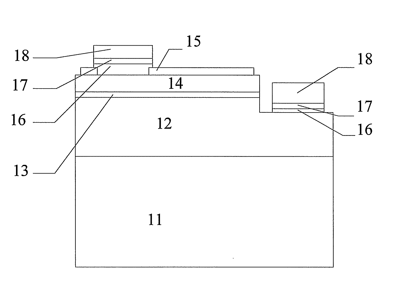
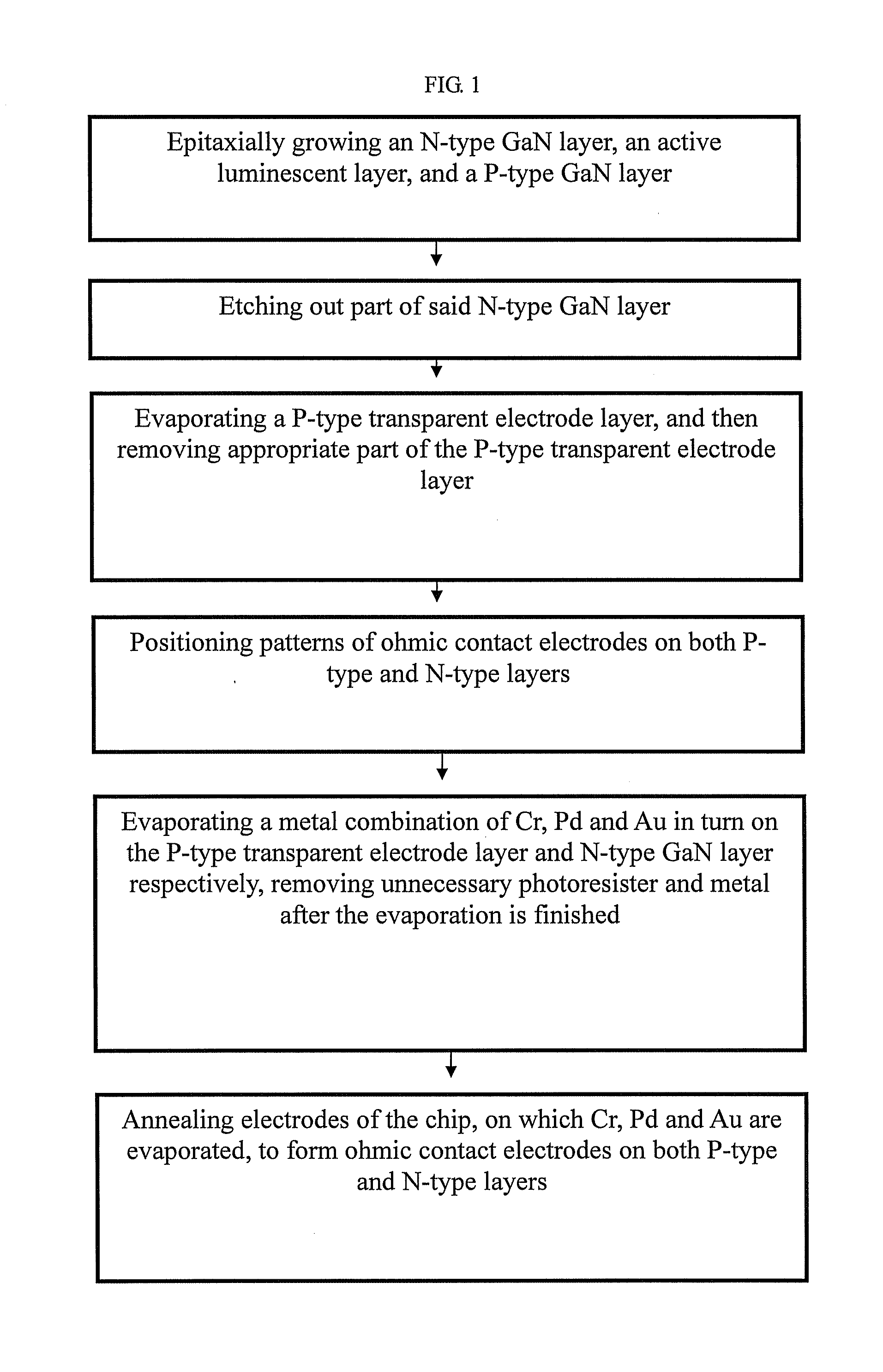
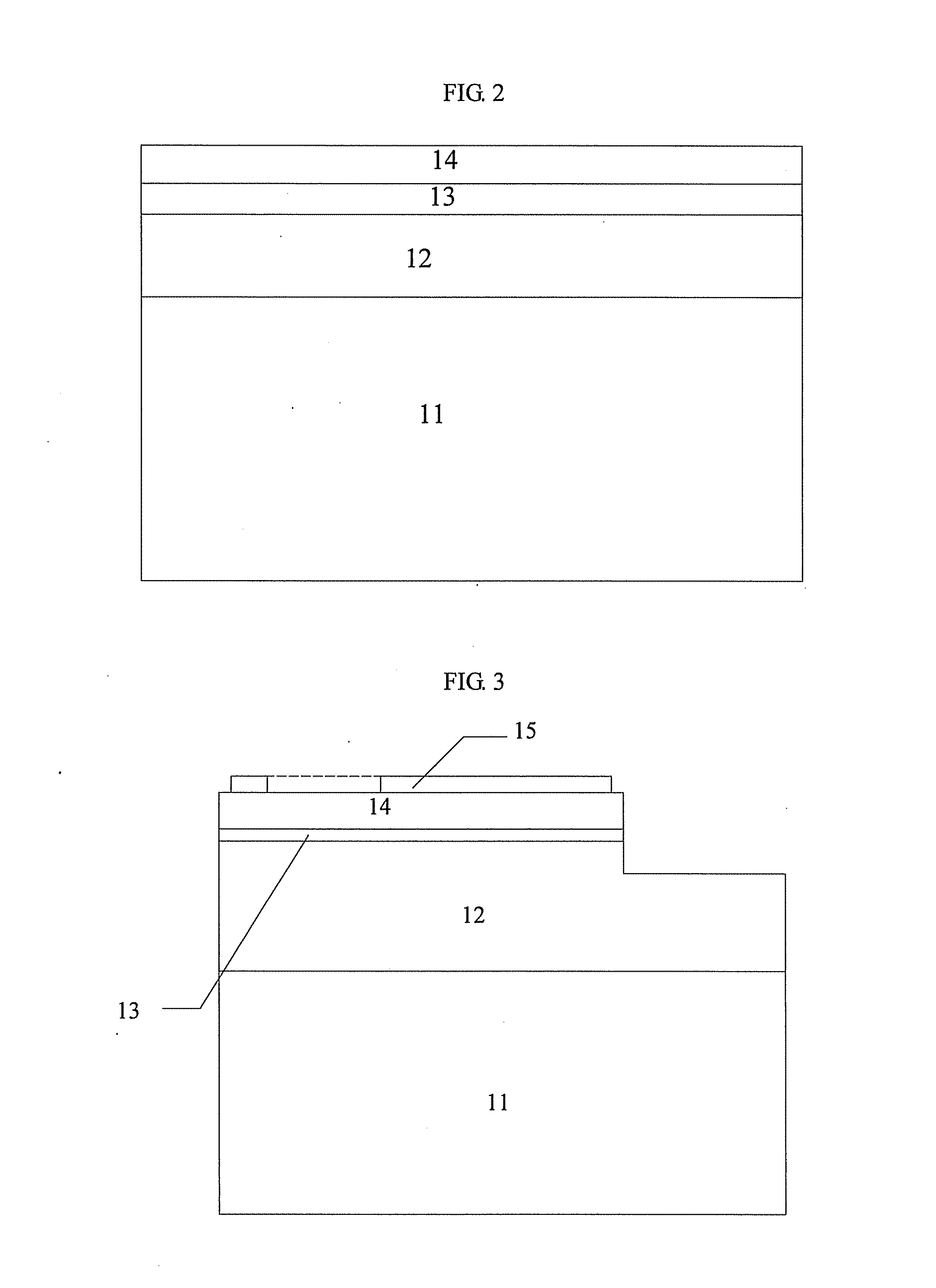
[0032]FIG. 1 is a fabrication flow chat of a set of ohmic contact electrodes on both P-type and N-type layers of a GaN-based LED according the present invention. FIG. 2 is a sectional view of the epitaxial structure of GaN-based LED chip on a sapphire substrate. FIG. 3 is a schematic view of etching out part of N-type layer on the epitaxial structure of chip and forming P-type transparent electrode layer. FIG. 4 is a schematic view showing positioning of ohmic contact electrodes on both P-type and N-type layers which are to be evaporated. FIG. 5 is a structure scheme of ohmic contact electrodes on both P-type and N-type layers of a GaN-based LED fabricated by using a metal combination of Cr / Pd / Au.

[0033]As shown in FIG. 1-FIG. 5, a method for fabricating set of ohmic contact electrodes on both P-type and N-type layers of GaN-based LED according to the present disclosure generally comprises the following steps:[0034](1) epitaxially growing an N-type GaN layer 12, an active luminescent...

second embodiment

[0040]A method for fabricating a set of ohmic contact electrodes on both P-type and N-type layers of a GaN-based LED according to the present disclosure generally comprises the following steps:[0041](1) epitaxially growing an N-type GaN layer 12, an active luminescent layer 13, and a P-type GaN layer 14 on a sapphire substrate 11;[0042](2) etching out part of the N-type GaN layer 12 with a plasma etcher;[0043](3) evaporating a P-type transparent electrode layer 15 on the surface of the P-type GaN layer 14 at a vacuum degree of 9.99×10⁻⁷ Torr, and then removing an appropriate part of a P-type transparent electrode layer 15 by photolithography and etching to prepare for evaporating an ohmic contact electrode in the next step;[0044](4) coating photoresister 19 on the surface of an epitaxial structure of chip by high speed spin-coating, then baking it until it is semi-dry, and using photomasks of a P-electrode and an N-electrode as a mask to photolithograph and develop the P-type transp...

third embodiment

[0047]A method for fabricating a set of ohmic contact electrodes on both P-type and N-type layers of a GaN-based LED according to the present disclosure generally comprises the following steps:[0048](1) epitaxially growing an N-type GaN layer 12, an active luminescent layer 13, and a P-type GaN layer 14 on a sapphire substrate 11;[0049](2) etching out part of the N-type GaN layer 12 with a plasma etcher;[0050](3) evaporating a P-type transparent electrode layer 15 on the surface of the P-type GaN layer 14 at a vacuum degree of 9.99×10⁻⁷ Torr, and then removing appropriate part of P-type transparent electrode layer 15 by photolithography and etching to prepare for evaporating ohmic contact electrode in the next step;[0051](4) coating photoresister 19 on the surface of an epitaxial structure of chip by high speed spin-coating, then baking it until it is semi-dry, and using photomasks of P-electrode and N-electrode as mask to photolithograph and develop P-type transparent electrode lay...


PUM

PropertyMeasurementUnit
P-type transparentaaaaaaaaaa
thicknessaaaaaaaaaa
temperatureaaaaaaaaaa

Abstract

The present disclosure relates to set of a ohmic contact electrodes on both P-type and N-type layers of a GaN-based light emitting diode (LED) and a fabricating method thereof. The materials of ohmic contact electrodes on both P-type and N-type layers of a GaN-based LED are a metal combination of Cr/Pd/Au. In one embodiment, the fabricating method comprises etching out an N-type GaN layer on an epitaxial structure on a sapphire substrate, and evaporating a P-type transparent electrode layer on the P-type GaN layer, then positioning patterns of the ohmic contact electrodes on both P-type and N-type layers, and then evaporating a metal combination of a Cr layer 50 Å to 500 Å thick, a Pd layer 300 Å to 1000 Å thick and an Au layer 3000 Å to 20000 Å thick in turn on the P-type transparent electrode layer and N-type GaN layer respectively, and then annealing electrodes of the chip, on which the Cr, Pd and Au layers are evaporated in nitrogen atmosphere for 5 minutes to 20 minutes at a temperature from 200 degrees to 450 degrees. Excellent ohmic contact characteristics and better thermal stability are obtained as well as higher oxidation resistance, thus improving the reliability of diode.

Description

CROSS-REFERENCE TO RELATED APPLICATIONS[0001]This application claims priority from Chinese Patent Application Serial No. 200710146312.3 filed Sep. 4, 2006, the disclosure of which, including the specification, drawings and claims, is incorporated herein by reference in its entirety.TECHNICAL FIELD[0002]The present disclosure pertains to the field of semiconductor technology, and more particularly, relates to a set of ohmic contact electrodes on both P-type and N-type layers of a GaN-Based light emitting diode (LED) and the fabricating method thereof.BACKGROUND ART[0003]Generally speaking, the contact behavior between metal and a semiconductor comprises ohmic contact and Schottky Contact. As to ohmic contact, the current-voltage relation on the contact interface shows linear characteristics, and compared with the resistance value of semiconductor itself, the contact resistance value between metal and semiconductor is almost negligible.[0004]At present, the popular materials for fabri...

Claims


Application Information

Patent Timeline
Patent Type & Authority Applications(United States)
IPC IPC(8): H01L33/00H01L33/32H01L33/40
CPCH01L33/40H01L33/32
Inventor CHAN, PHILIPWANG, RAYMONDLEI, LEO
Owner PODIUM PHOTONICS GUANGZHOU
Why Eureka
Try Eureka