Multilayer wiring substrate, method of manufacturing the same, and semiconductor device

a wiring substrate and multi-layer technology, applied in the direction of printed circuit manufacturing, printed circuit aspects, non-printed jumper connection addition, etc., can solve the problem that the radiation fin cannot be mounted, and achieve the effect of excellent electrical characteristics, good impedance matching, and low impedan

Inactive Publication Date: 2009-03-19
SHINKO ELECTRIC IND CO LTD
View PDF1 Cites 3 Cited by
  • Summary
  • Abstract
  • Description
  • Claims
  • Application Information

AI Technical Summary

Benefits of technology

[0010]It is an aspect of the present invention to provide a multilayer wiring substrate capable of greatly relaxing the channel problem about the high-density multi-I/O rerouting in excess of thousands or more. Further, it is another aspect of the present invention to provide a multilayer wiring substrate capable of exhibiting excellent electrical characteristics typifie...

Problems solved by technology

However, when the wiring substrate is formed of the multilayer wiring substrate, such multilayer wiring substrate is constructed such that an elec...

Method used


Image

  • Multilayer wiring substrate, method of manufacturing the same, and semiconductor device
  • Multilayer wiring substrate, method of manufacturing the same, and semiconductor device
  • Multilayer wiring substrate, method of manufacturing the same, and semiconductor device

Examples


example

[0069]Subsequently, the present invention will be described with reference to an example. In this event, the present invention is never limited to the following example.

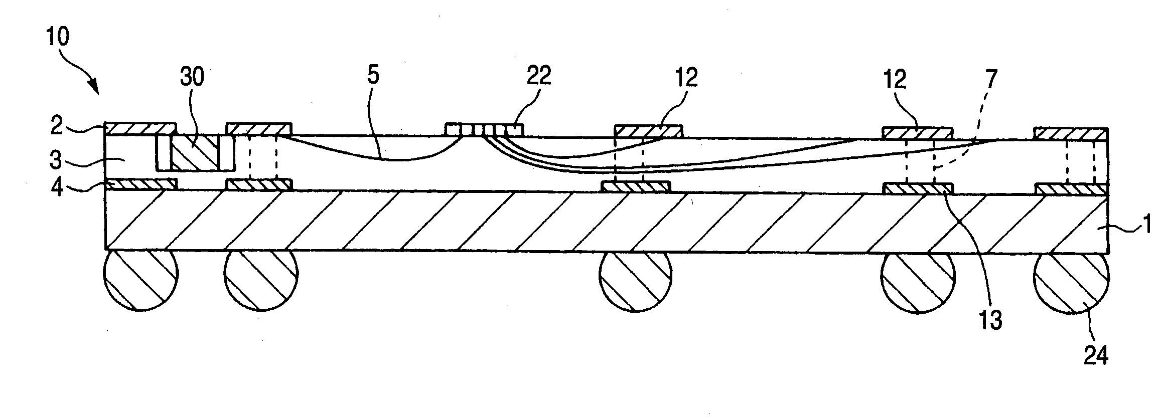
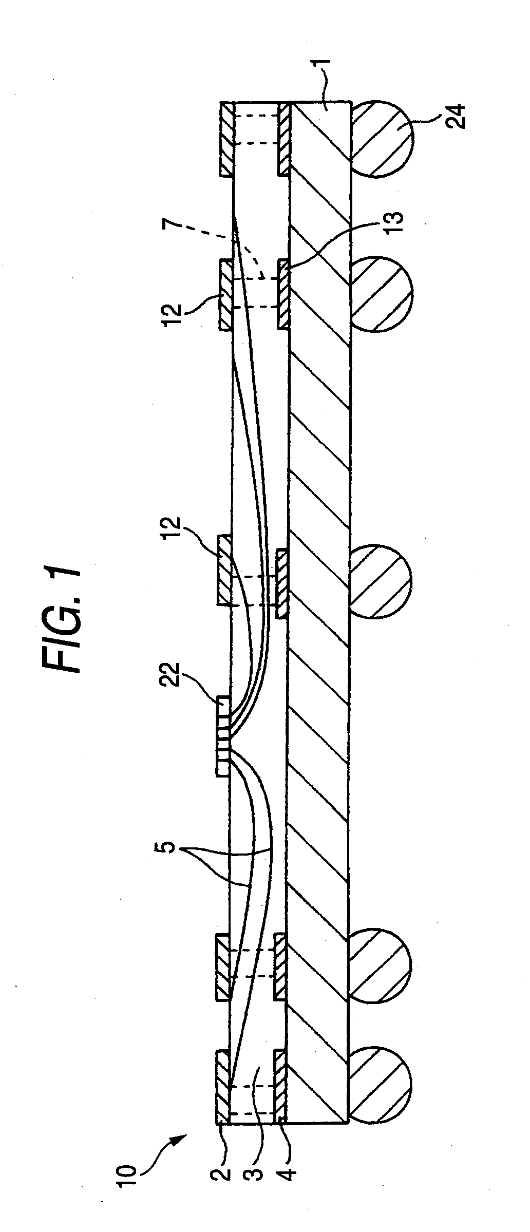
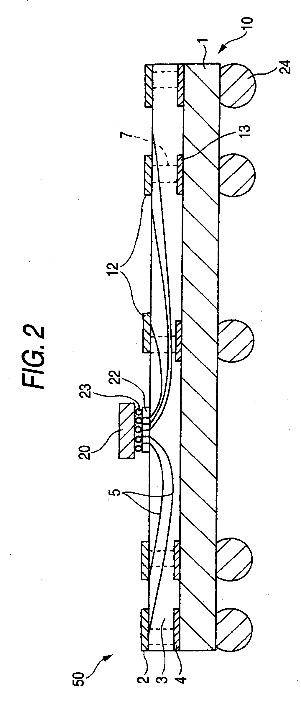
[0070]A copper foil on which alignment marks are formed (size: about 15 cm square) was prepared. Two spots on the pad surface of this copper foil were connected via a gold wire of 20 μm diameter in plural predetermined locations respectively. Then, the three-fluid epoxy resin was supplied by the potting to cover the copper foil and the gold wires entirely, and thus a resin layer that can cover the gold wires completely (thickness: about 30 μm on the copper foil) was formed. The resin layer was cured while holding at a temperature of 50 to 100° C. Then, the through holes each having an about 80 μm diameter were formed in predetermined positions by the CO2 laser. In turn, a copper is filled in the through holes by applying the electroless copper plating or the electrolytic copper plating to the whole surface of the res...


PUM


Abstract

There is provided a multilayer wiring substrate on which at least one semiconductor element is mounted. The multilayer wiring substrate includes: a baseboard; a first wiring layer formed on the baseboard and having a plurality of first wiring portions; an insulating layer formed on the baseboard; a second wiring layer formed on the insulating layer and having a plurality of second wiring portions, the second wiring portions being electrically connected to each other via a conductor wire, the conductor wire being arranged within the insulating layer three-dimensionally in a curved manner; and conductor portions configured to pass through the insulating layer and connecting the first wiring portions and the second wiring portions.

Description

[0001]This application is based on and claims priority from Japanese Patent Application No. 2007-231692, filed on Sep. 6, 2007, the entire contents of which are hereby incorporated by reference.BACKGROUND OF THE INVENTION[0002]1. Technical Field[0003]The present disclosure relates to a multilayer wiring substrate and, more particularly, to a multilayer wiring substrate capable of exhibiting excellent electrical characteristics typified by low impedance, good impedance matching, low crosstalk, etc. and solving the problem of heat radiation, and a method of manufacturing the same. Also, the present disclosure relates to a semiconductor device using the multilayer wiring substrate.[0004]2. Related Art[0005]With the progress of miniaturization and higher functionality of the semiconductor device in recent years, the number of electrode terminals of the semiconductor element mounted on the semiconductor device (referred to as the “semiconductor chip” hereinafter) is increasing. In order ...

Claims


Application Information

Patent Timeline
IPC IPC(8): H01L23/495H01L21/00
CPCH01L21/4857H01L21/6835H01L23/49816H01L23/49838H01L23/49861H01L24/45H01L24/48H01L2221/68345H01L2223/6611H01L2224/16H01L2224/45015H01L2224/45124H01L2224/45139H01L2224/45144H01L2224/45147H01L2224/45155H01L2224/48091H01L2224/484H01L2224/48599H01L2224/48699H01L2224/73204H01L2224/85455H01L2224/85464H01L2924/01002H01L2924/01004H01L2924/01005H01L2924/01013H01L2924/01027H01L2924/01028H01L2924/01029H01L2924/01046H01L2924/01047H01L2924/0105H01L2924/01078H01L2924/01079H01L2924/01082H01L2924/014H01L2924/14H01L2924/15192H01L2924/15311H01L2924/19041H01L2924/19051H01L2924/19107H01L2924/20753H01L2924/30105H01L2924/30107H01L2924/3011H05K3/222H05K3/4046H05K3/4614H05K3/4652H05K2201/10234H05K2201/10287H05K2203/0733H01L2924/01006H01L2924/01019H01L2924/01033H01L2924/01076H01L2924/07802H01L2224/16235H01L2924/00014H01L2924/20752H01L2924/00H01L2224/48855H01L2224/48864H01L2224/48655H01L2224/48664H01L2224/48755H01L2224/48764
Inventor HORIUCHI, MICHIOKATAGIRI, FUMIMASASUGANUMA, SHIGEAKITOKUTAKE, YASUEYOSHIKE, JUN
Owner SHINKO ELECTRIC IND CO LTD
Why Eureka
Try Eureka