

Semiconductor device and method for manufacturing the same, and electric device
a semiconductor and semiconductor technology, applied in the field of semiconductor devices, can solve the problems of complex process and high target cost, and achieve the effect of high circuit integration and simplified steps
- Summary
- Abstract
- Description
- Claims
- Application Information
AI Technical Summary
Benefits of technology
Problems solved by technology
Method used
Image

Examples
embodiment mode 1
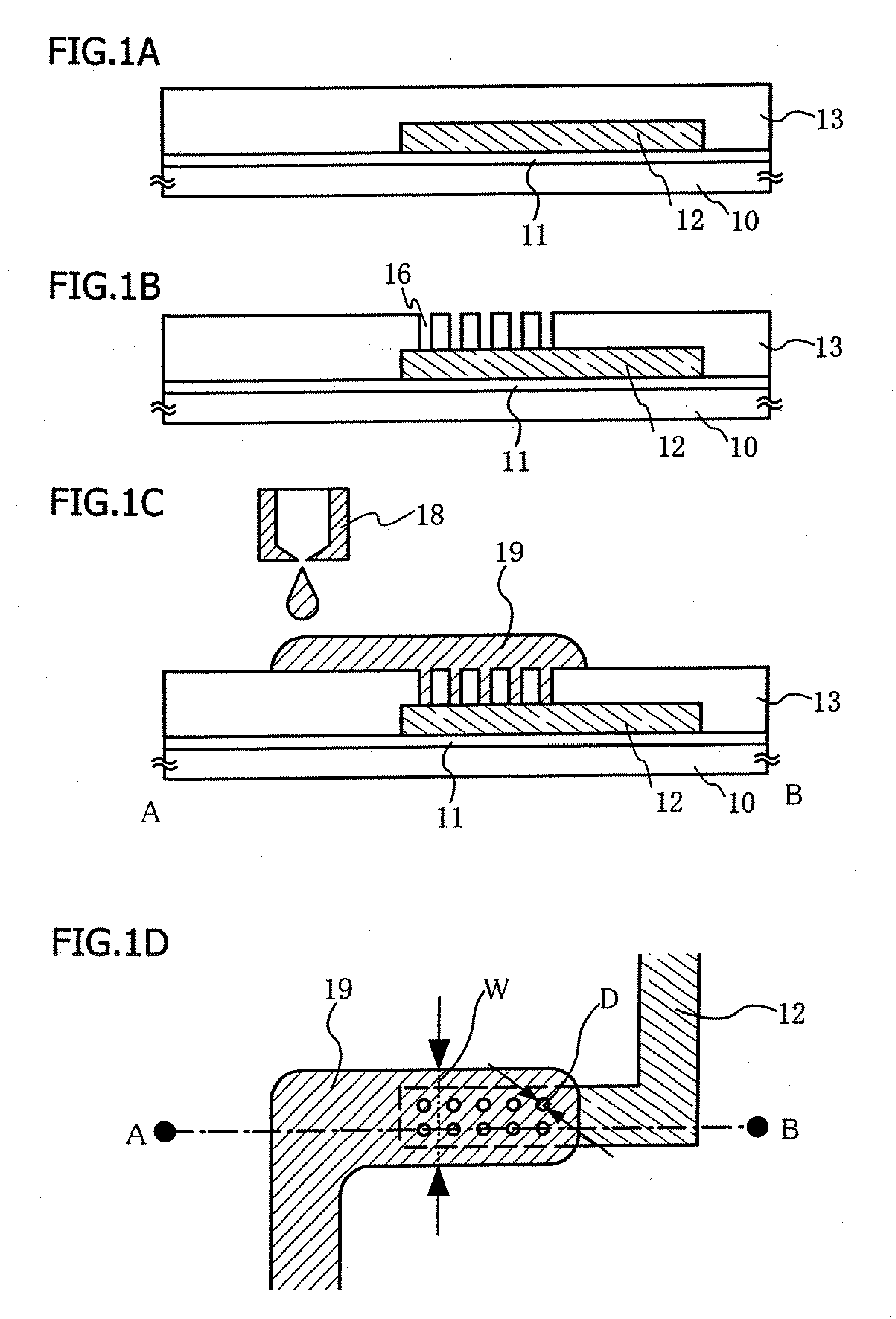
[0097]In this embodiment mode, a method for forming a contact hole in a first conductive layer and a method for forming a second conductive layer electrically connected to the first conductive layer through the contact hole will be explained with reference to FIGS. 1A to 1D, FIGS. 2A and 2B, FIG. 10, and FIG. 11.
[0098]First, a base insulating film 11 is formed over a substrate 10 having an insulating surface, and a first conductive layer 12 is formed over the base insulating film 11. Next, an insulating film 13 covering the first conductive layer 12 is formed. A cross-sectional view of this stage is shown in FIG. 1A.
[0099]Note that a glass substrate or quartz substrate having light transparency is preferably used as the substrate 10 having an insulating surface.
[0100]In addition, as for the base insulating film 11, a base film made of an insulating film such as a silicon oxide film, a silicon nitride film, or a silicon oxynitride film is formed. Herein, an example where a two-layer ...
embodiment mode 2
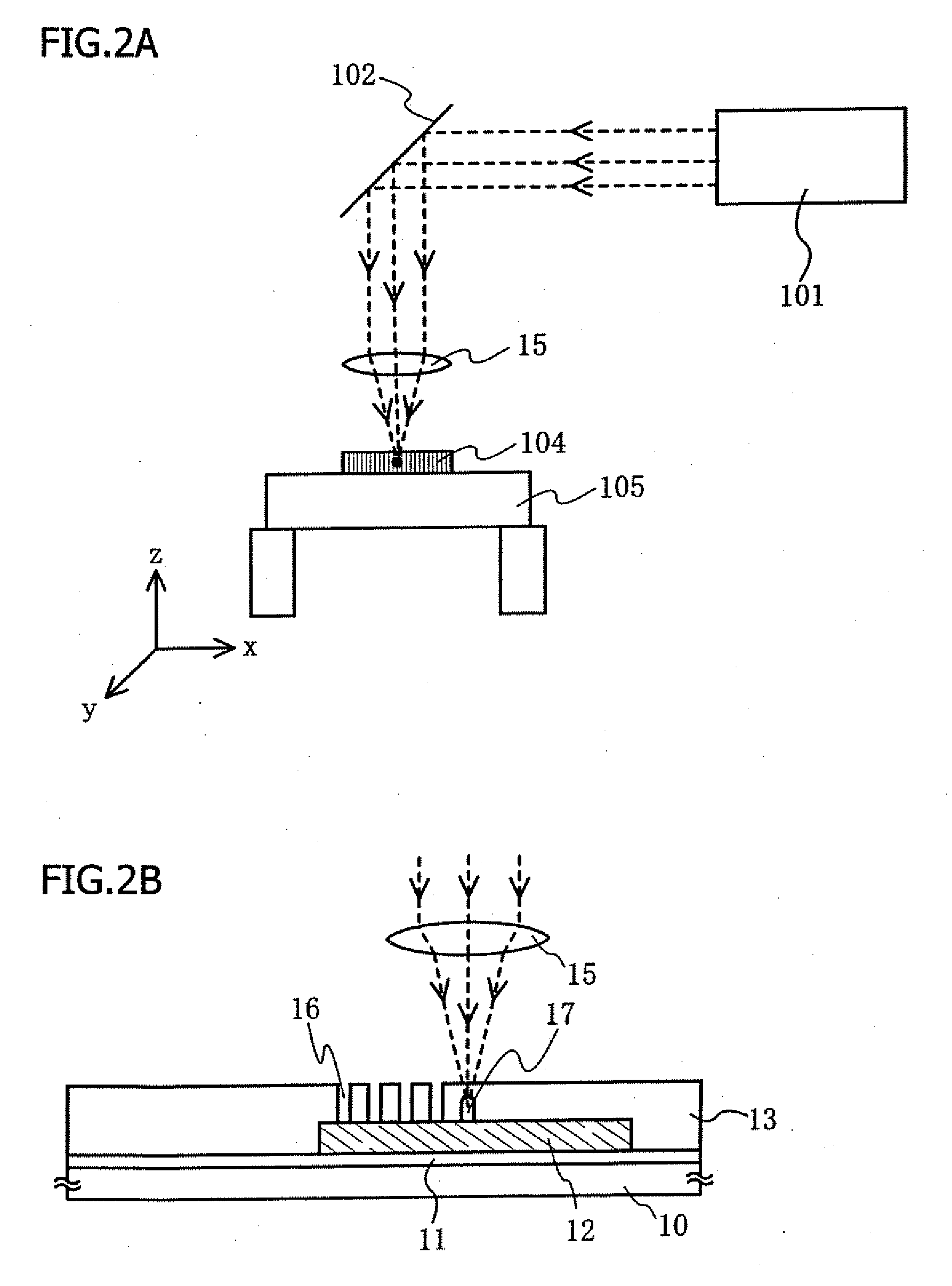
[0126]In this embodiment mode, an example of an opening the cross-sectional shape of which differs from Embodiment Mode 1 will be shown with reference to FIGS. 3A to 3C. Portions different from Embodiment Mode 1 will be explained in detail and portions identical with FIGS. 1A to 1D in FIGS. 3A to 3C are denoted by the same reference numerals.
[0127]Note that a cross-sectional shape of an opening in FIGS. 1A to 1D is shown in a columnar shape; however, the present invention is not limited thereto and an opening the shape of which has a structure in which a plurality of openings is connected to each other in an insulating film as shown in FIG. 3 may be employed.
[0128]First, as well as in Embodiment Mode 1, a base insulating film 11 and a first conductive layer 12 are formed over a substrate 10 having an insulating surface.
[0129]Next, after forming an insulating film made of a material that is light transmitting to laser light having a pulse width of 10−4 seconds to 10−2 seconds, an ins...
embodiment mode 3
[0140]In this embodiment mode, an example of forming a plurality of openings with the combination of laser light and etching will be explained with reference to FIGS. 4A to 4C. Portions different from Embodiment Mode 1 will be explained in detail, and portions identical with FIGS. 1A to 1D are denoted by the same reference numerals in FIGS. 4A to 4C.
[0141]After forming an insulating film made of a material that is light transmitting to laser light having a pulse width of 10−4 seconds to 10−2 seconds, an insulating film 33 having a closed pore 37 is obtained by irradiation of ultrashort pulsed laser light. When an ultrashort pulsed laser is condensed in the insulating film, multiphoton absorption can occur only at a condensed spot where the ultrashort pulsed laser is condensed, a closed pore can be formed, and one penetrating opening can be formed by moving the condensed spot. When the pulsed width of the laser light is 10−4 seconds to 10−2 seconds, the laser light is not absorbed by...
PUM
 Abstract
Description
Claims
Application Information