Photoelectric conversion element and imaging device

a conversion element and photoelectric technology, applied in the direction of thermoelectric device junction materials, semiconductor devices, electrical apparatus, etc., can solve the problems of low light utilization efficiency, reduced area of the photo diode portion, and reduced aperture ratio, so as to achieve high photoelectric conversion efficiency and low dark current. , the effect of high speed respons

Active Publication Date: 2009-04-02
FUJIFILM CORP
View PDF4 Cites 22 Cited by
  • Summary
  • Abstract
  • Description
  • Claims
  • Application Information

AI Technical Summary

Benefits of technology

[0010]An object of the present invention is to provide a photoelectric conversion element and a solid-state imaging device, which includes an organic material and which can show a high photoelectric conversion efficiency, a low dark current, and a high-speed response properties.

Problems solved by technology

However, in this system, each of the color filters transmits only light of a particular wavelength, and light not transmitting through the color filter is not utilized, and thus light-utilizing efficiency is bad.
Also, with the recent increase in number of pixels, the size of pixel becomes smaller, which leads to reduction in area of the photo diode portion, reduction in aperture ratio, and reduction in light-collecting efficiency.
However, the absorption ranges utilizing the difference in the depth direction of Si overlap with each other, which leads to insufficient color-separating properties, and thus color separation is poor.
However, no specific proposals have so far been made as to what would be such organic photoelectric conversion materials and element structure.

Method used


Image

  • Photoelectric conversion element and imaging device
  • Photoelectric conversion element and imaging device
  • Photoelectric conversion element and imaging device

Examples


first embodiment

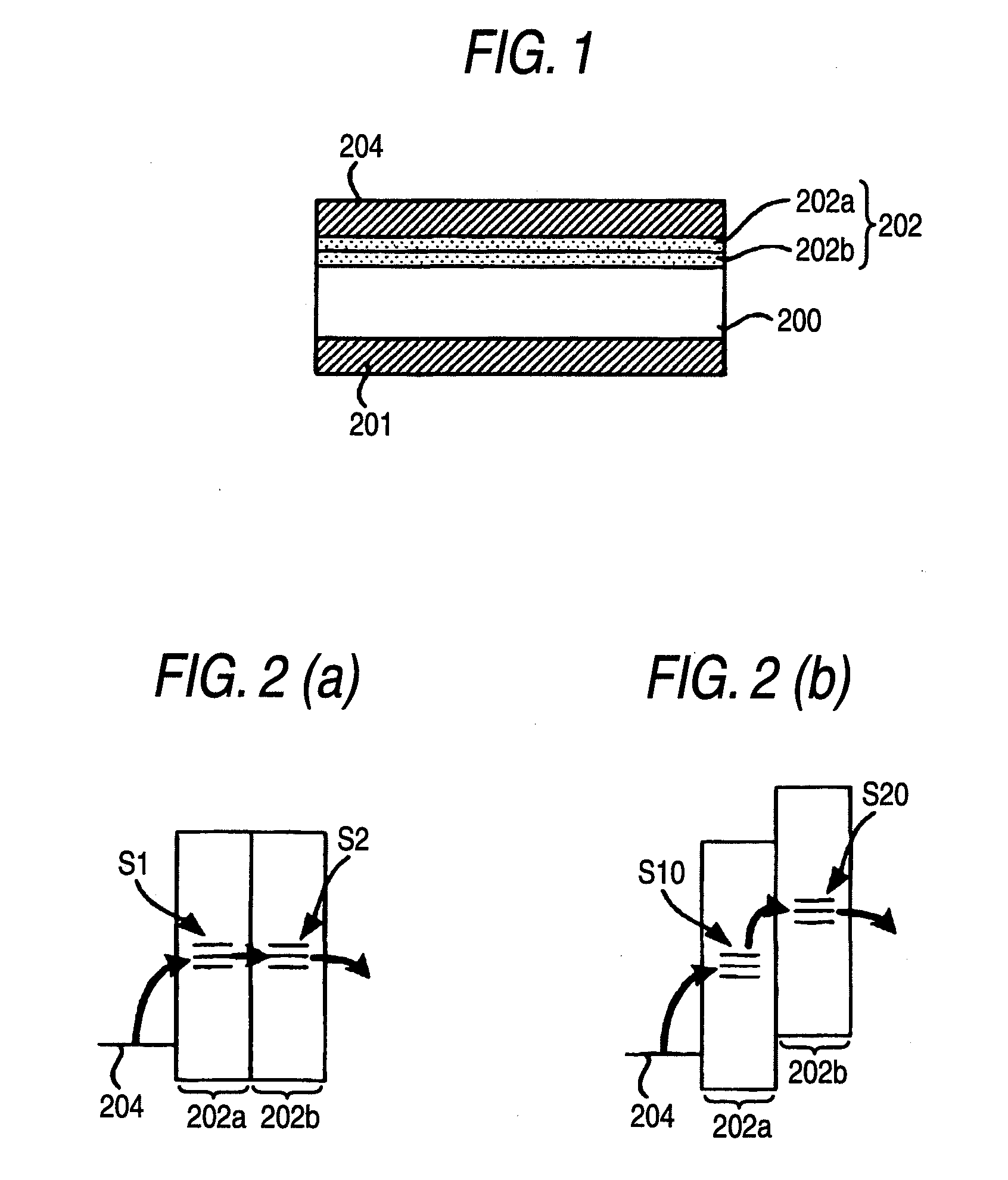
[0171]FIG. 1 is a cross-sectional schematic view showing a constitution of the photoelectric conversion element having the charge blocking layer of this embodiment.

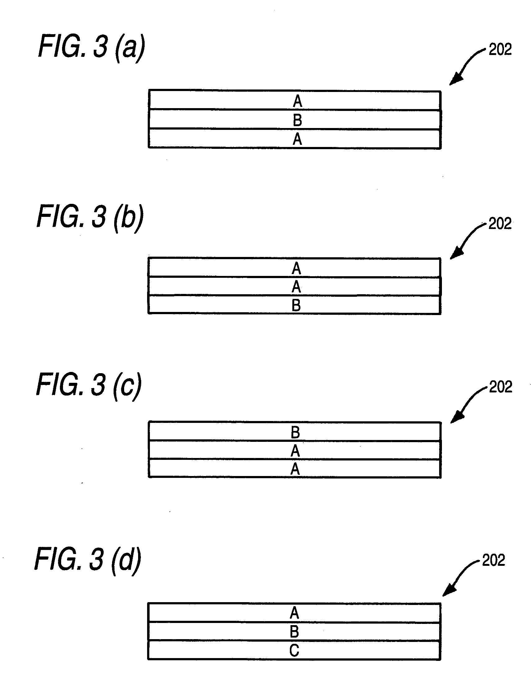
[0172]In FIG. 1, reference numeral 200 designates a photoelectric conversion layer, 202 designates a charge blocking layer of two-layer structure, 202a and 202b designate layers constituting the charge blocking layer 202, and 201 and 204 each designates an electrode.

[0173]For example, when the electrode 204 serves as an electrode on the light incident side, the electrode 204 is preferably constituted by a material having a high transparency since it is necessary to introduce light into the photoelectric conversion layer 200 through the electrode. As an electrode having a high transparency, there is illustrated a transparent conductive oxide (TCO). Also, preferably, the electrode 201 is likewise constituted by a material having a high transparency since, as will be seen in the constitution of the imaging device to be descr...

second embodiment

[0206]In this embodiment, a specific example of a photoelectric conversion element having a charge blocking layer of the plural-layer structure will be described by reference to FIGS. 6 to 11.

[0207]The charge blocking layer includes “a hole blocking layer” which has a large barrier for hole injection from the adjacent electrode and “an electron blocking layer” which has a large barrier for electron injection from the adjacent electrode a high ability of transporting holes which are a carrier of photocurrent. In organic light-emitting elements, a blocking layer using an organic material has already been used in order to prevent penetration of the carrier through a light-emitting layer, as is described in JP-A-11-339966 and JP-A-2002-329582. By sandwiching such organic blocking layer between the electrode and the photoelectric conversion layer in the photoelectric conversion portion, the photoelectric conversion efficiency and the response speed can be improved without reduction of th...

third embodiment

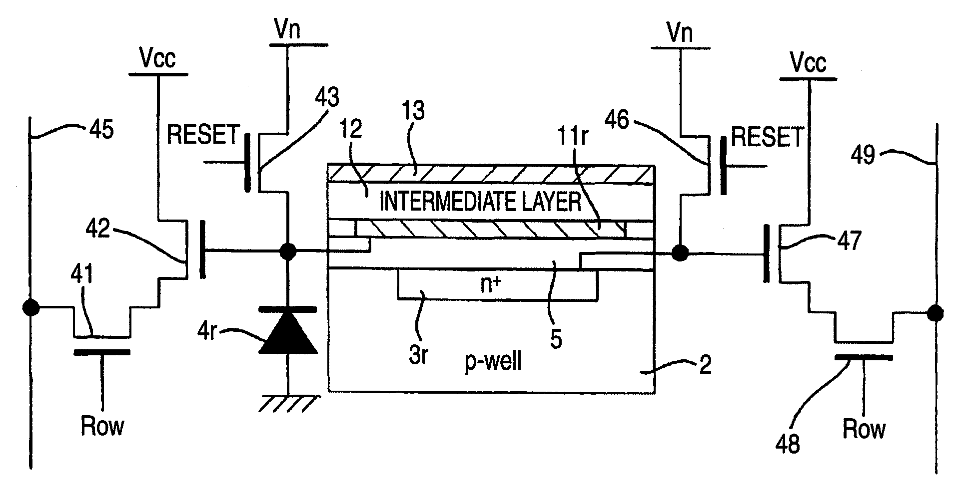
[0241]An example of the constitution of an imaging device using the photoelectric conversion element of the structure shown in FIG. 11 will be described below. In the following descriptions, reference is made to FIGS. 12 to 16. In each drawing, both the hole blocking layer and the electron blocking layer have a plural-layer structure as is the same with the above-described embodiment. However, for drawing convenience, each blocking layer is not drawn as separate plural layers in FIG. 12 to 16.

[0242]FIG. 12 is a cross-sectional schematic view showing one pixel of a solid-state imaging device for illustrating the third embodiment of the invention. FIG. 13 is a cross-sectional schematic view of an intermediate layer shown in FIG. 12. In this solid-state imaging device, a number of pixels shown in FIG. 12 are arranged on the same plane in an array pattern, and data on one pixel of an image data can be generated by a signal obtained from the one pixel.

[0243]One pixel of the solid-state i...


PUM


Abstract

A photoelectric conversion element is provided and includes: a conductive thin layer; an organic photoelectric conversion layer including a compound represented by formula (I); and a transparent conductive thin layer, in this order:
In the formula (I), X represents O, S or N—R10; Rx and Ry each independently represents a hydrogen atom or a substituent, at least one of Rx and Ry is an electron-withdrawing group, and Rx and Ry may be connected to each other to form a ring, provided that Rx and Ry do not represent a cyano group at the same time; R7 to R10 each independently represents a hydrogen atom or a substituent, and R8 and R9 may be connected to each other to form a ring; L represents a linking group comprising a conjugated bond; and D1 represents a group of atoms.

Description

[0001]This application is based on and claims priority under 35 U.S.C. §119 from Japanese Patent Application No. 2007-256731 filed Sep. 28, 2007, the entire disclosure of which is herein incorporated by reference.BACKGROUND OF THE INVENTION[0002]1. Field of the Invention[0003]The present invention relates to a solid-state imaging device in which an organic photoelectric conversion portion is formed on a charge accumulation / transfer / read-out substrate, and provides a solid-state imaging device showing high S / N and a high response speed by specifying a structure of the material.[0004]2. Description of Related Art[0005]Visible light sensors are generally devices prepared by forming a photoelectric conversion site through formation of PN junction within a semiconductor such as Si and, as a solid-state imaging device, a plane type light-receiving device is being widely used in which photoelectric conversion sites are two-dimensionally arranged within a semiconductor, and signals each cor...

Claims


Application Information

Patent Timeline
Patent Type & Authority Applications(United States)
IPC IPC(8): H01L51/30
CPCH01L51/001H01L51/0051H01L51/424H01L51/0081H01L51/0059H10K71/164H10K85/611H10K85/631H10K85/324H10K30/20
Inventor MITSUI, TETSURONOMURA, KIMIATSUNII, KAZUMI
Owner FUJIFILM CORP
Why Eureka
Try Eureka