Capacitor and method of manufacturing the same

a technology of capacitors and manufacturing methods, applied in the field of capacitors, can solve the problems of difficult to obtain pillar-shaped bodies having uniform section and desired length, and difficult to achieve large-capacity with increase of an area. , to achieve the effect of improving the selectivity of dielectric materials and electrode metals, improving the selectivity of capacitors, and simplifying the manufacturing process

Active Publication Date: 2009-04-02
TAIYO YUDEN KK
View PDF9 Cites 26 Cited by
  • Summary
  • Abstract
  • Description
  • Claims
  • Application Information

AI Technical Summary

Benefits of technology

[0008]To overcome at least one of the above problems, it is an object of at least one embodiment of the invention to provide a capacitor and a method of manufacturing the same, which are capable of achieving miniaturization and increase of capacitance density of the capacitor, improvement of selectivity of dielectric material and electrode metal in constructing the capacitor, and simplification of a manufacturing process of the capacitor.
[0010]With this configuration, since the electrodes are formed in the holes passing through the dielectric layer in the thickness direction of the dielectric layer and the first electrodes (for example, positive poles) and the second electrodes (for example, negative poles) are randomly distributed on the conductive layers on the front and rear surfaces of the dielectric layer, it is possible to increase an area defining a capacitance and hence achieve large-capacity of a capacitor.
[0013]With this configuration, since the structure body of the dielectric layer is first formed and the gap (hole) is later filled with the electrode material, it is possible to improve selectivity of electrode metal and achieve simplification of a manufacturing process.
[0016]With this configuration, with the structure body of the oxide substrate, which is made of anodic oxide of metal and has a plurality of holes, as a mold, since the electrodes are formed in the plurality of holes of the dielectric layer while transferring any structure body into the dielectric layer, and the first electrodes (for example, positive poles) and the second electrodes (for example, negative poles) are randomly distributed on the conductive layers on the front and rear surfaces of the dielectric layer, it is possible to increase an area defining a capacitance and hence achieve large-capacity of a capacitor. In addition, since the gap of the structure body of the oxide substrate formed by the anodization is later filled with the electrode material, it is possible to improve selectivity of electrode metal and achieve simplification of a manufacturing process. Further, since the oxide substrate is removed and the gap is filled with any dielectric material, it is possible to improve selectivity of dielectric material and alter dielectric material depending on use of a capacitor.

Problems solved by technology

An Al electrolytic capacitor uses electrolyte and so has a challenge to a structure to allow for prevention of liquid leakage.
A multi-layer ceramic capacitor requires firing and has a challenge to a design in consideration of variation of a difference in thermal contraction between an electrode and a dielectric substance.
However, the above related art have the following problems.
S61-29133 disclosing the structure in which the grain boundary-insulated semiconductor ceramic with the plurality of through-holes is used as a dielectric layer and the capacitive electrode bodies are selectively inserted in the through-holes, it is difficult to achieve large-capacity with increase of an area due to difficulty of micro-processing.
In the technique disclosed in JP-A No. 2003-249417, since electrode material is attached to the porous substrate used as the mask and holes are enlarged when the porous substrate is etched, it is difficult to obtain the pillar-shaped bodies having uniform section and desired length.
In addition, when the pillar-shaped bodies become lengthened, there may occur variation in film thickness of the dielectric thin film, which makes it difficult to achieve large-capacity with increased height of the pillar-shaped bodies.

Method used


Image

  • Capacitor and method of manufacturing the same
  • Capacitor and method of manufacturing the same
  • Capacitor and method of manufacturing the same

Examples


embodiment 1

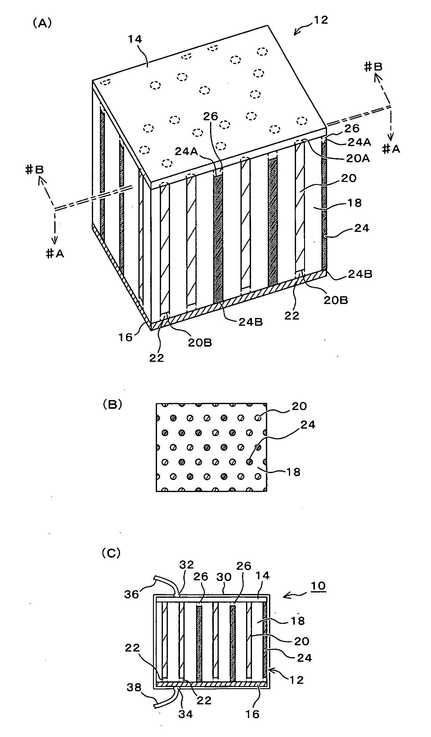
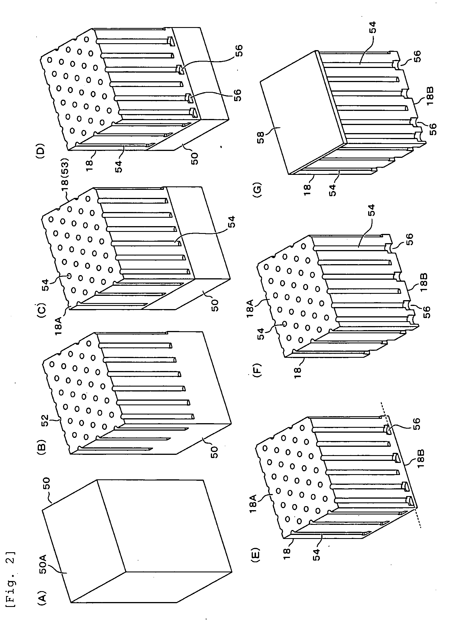
[0035]First, Embodiment 1 of the present invention will be described with reference to FIGS. 1 to 5. FIG. 1A is a perspective view showing an external appearance of a capacitor element according to Embodiment 1, FIG. 1B is a sectional view taken along line #A-#A and viewed in an arrow direction in FIG. 1A, and FIG. 1C is a sectional view of a capacitor according to Embodiment 1, which is taken along line #B-#B and viewed in an arrow direction in FIG. 1A. FIGS. 2 to 4 are views showing exemplary manufacturing processes of Embodiment 1, and FIG. 5 shows a SEM image having a two dimensional section observed in the course of manufacturing the capacitor element of Embodiment 1.

[0036]A capacitor 10 of this embodiment is configured with a capacitor element 12 as a main component, as shown in FIG. 1. The capacitor element 12 includes a pair of conductive layers 14 and 16 which are opposed to each other at a predetermined interval, a dielectric layer 18 interposed between the conductive laye...

embodiment 2

[0050]Next, Embodiment 2 of the present invention will be described with reference to FIGS. 6 to 8. FIG. 6 is a perspective view showing an external appearance of a capacitor element according to this embodiment, and FIGS. 7 to 8 are views showing exemplary manufacturing processes of this embodiment. In these figures, the same components as Embodiment 1 are denoted by the same reference numerals. As shown in FIG. 6, a capacitor element 100 of this embodiment includes a pair of opposing conductive layers 102 and 104, a dielectric layer 106 which is made of high permittivity material and is interposed between the pair of conductive layers 102 and 104, and a plurality of first electrodes 108 and second electrodes 112 with which a plurality of holes formed in the dielectric layer are filled.

[0051]The first electrodes 108 and the second electrodes 112 are randomly distributed like Embodiment 1. An insulation cap 110 is formed between one end portion 108A of each of the first electrode 10...


PUM

PropertyMeasurementUnit
aspect ratioaaaaaaaaaa
thicknessaaaaaaaaaa

Abstract

A capacitor element includes a pair of conductive layer, a plurality of first electrodes and second electrodes, and insulation caps for insulating these electrodes from the conductive layers. By anodizing a metal substrate in two stages, holes filled with the first electrodes and holes filled with the second electrodes are randomly distributed

Description

BACKGROUND OF THE INVENTION[0001]1. Field of the Invention[0002]The present invention relates to a capacitor and a method of manufacturing the same, and more particularly, to increase of capacitance density of a capacitor, improvement of selectivity of dielectric material and electrode metal in constructing the capacitor, and simplification of a manufacturing process of the capacitor.[0003]2. Description of the Related Art[0004]Al electrolytic capacitors and multi-layer ceramic capacitors have been known and widely used in the art. An Al electrolytic capacitor uses electrolyte and so has a challenge to a structure to allow for prevention of liquid leakage. A multi-layer ceramic capacitor requires firing and has a challenge to a design in consideration of variation of a difference in thermal contraction between an electrode and a dielectric substance. Examples of techniques for implementing small and large-capacity capacitors may include a grain boundary-insulated semiconductor ceram...

Claims


Application Information

Patent Timeline
Patent Type & Authority Applications(United States)
IPC IPC(8): H01G4/005
CPCH01G4/302H01G4/232Y10T29/43H01G9/048H01G9/07H01G4/012Y10T29/435
Inventor MASUDA, HIDETOSHIIRIEDA, TAISEIKUROSAWA, MASARUMIZUNO, KOTARO
Owner TAIYO YUDEN KK
Why Eureka
Try Eureka