Belt-shaped mold and nanoimprint system using the belt-shaped mold

a technology of nano-imprinting and belt-shaped molds, which is applied in the direction of photomechanical equipment, manufacturing tools, instruments, etc., can solve the problems of increasing the cost of associated systems, requiring an extended period, and difficult to fabricate such fine patterns using photolithography, and achieves rapid and stable formation and high aspect ratio.

Inactive Publication Date: 2009-04-02
HITACHI LTD
View PDF6 Cites 60 Cited by
  • Summary
  • Abstract
  • Description
  • Claims
  • Application Information

AI Technical Summary

Benefits of technology

[0012]Therefore, to resolve the above described shortcomings, one objective of the present invention is to provide a fine pattern transfer, belt-shaped mold, with which a fine structure having a high aspect ratio can formed rapidly and stably using nanoimprinting, and a fine pattern transfer system (a nanoimprint system) that employs this mold.

Problems solved by technology

However, in consonance with developments in the structural refinement and the integration of circuits, required element sizes have been reduced until they are the equivalent of the wavelengths of light sources used for photolithography exposure, and fabricating such fine patterns using photolithography is difficult.
However, a fundamental disadvantage of the direct writing method is that whereas the time required to complete one pattern is normally not excessive, to complete a number of patterns an extended period is required, since the time needed would be a multiple of that for a single pattern.
However, with this system, when the situation is such that the refinement of patterns is continuous, associated system costs rise, i.e., the size of the electron beam lithography system is increased and accurate control means, for positioning the masks, must be provided.
However, the following problem has been identified for the above described nanoimprint technique for accurately forming a fine pattern.
Therefore, an extended period of time is required for one pattern imprinting cycle, and it is difficult for this method to be employed for the mass production of a fine structure.
Thus, the aspect ratio (the pattern height / the pattern width) for a pattern to be imprinted tends to be low, e.g., 0.086 (60 nm / 700 nm) or 0.57 (40 nm / 70 nm), and it is difficult to use this method for a device, such as an optical device or a bio-device, that requires a fine structure having a high aspect ratio (e.g., an aspect ratio of 1 or greater).
However, at present, since the maximum diameter of a sample wafer to be processed is substantially 300 mm, it is difficult for a fine pattern to be directly formed on a long, large dimension belt-shaped mold.

Method used


Image

  • Belt-shaped mold and nanoimprint system using the belt-shaped mold
  • Belt-shaped mold and nanoimprint system using the belt-shaped mold
  • Belt-shaped mold and nanoimprint system using the belt-shaped mold

Examples


embodiment 1

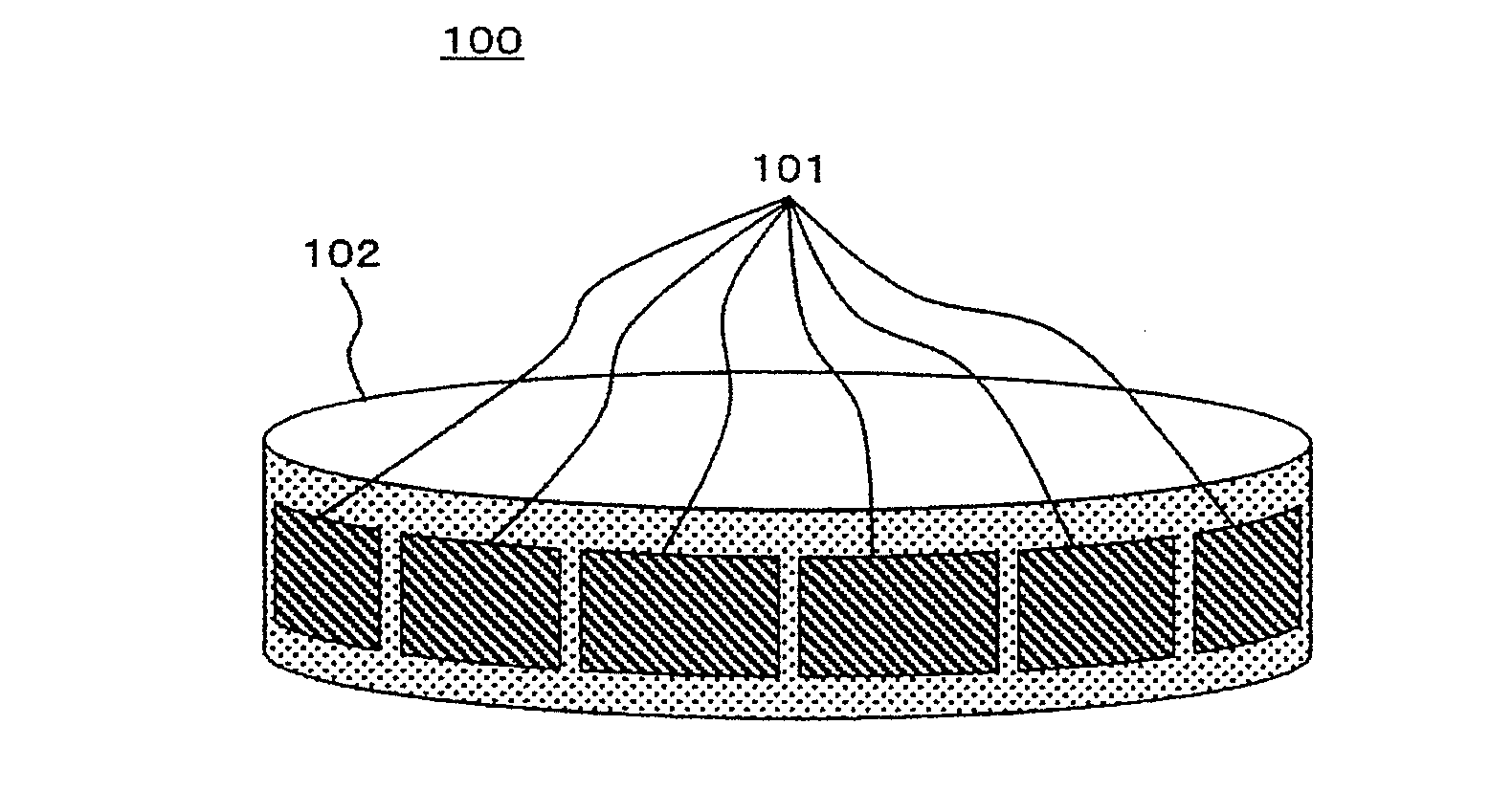
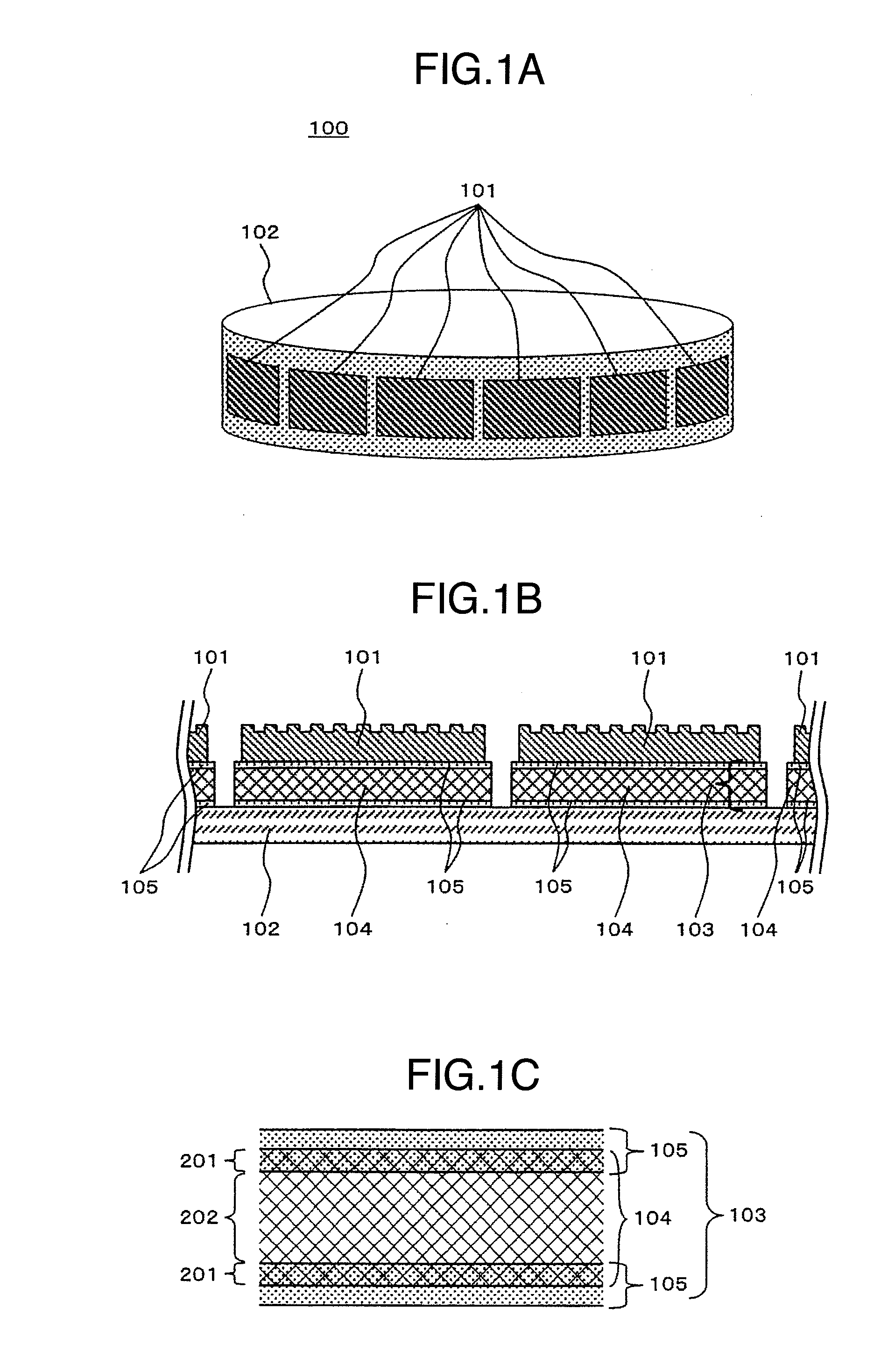
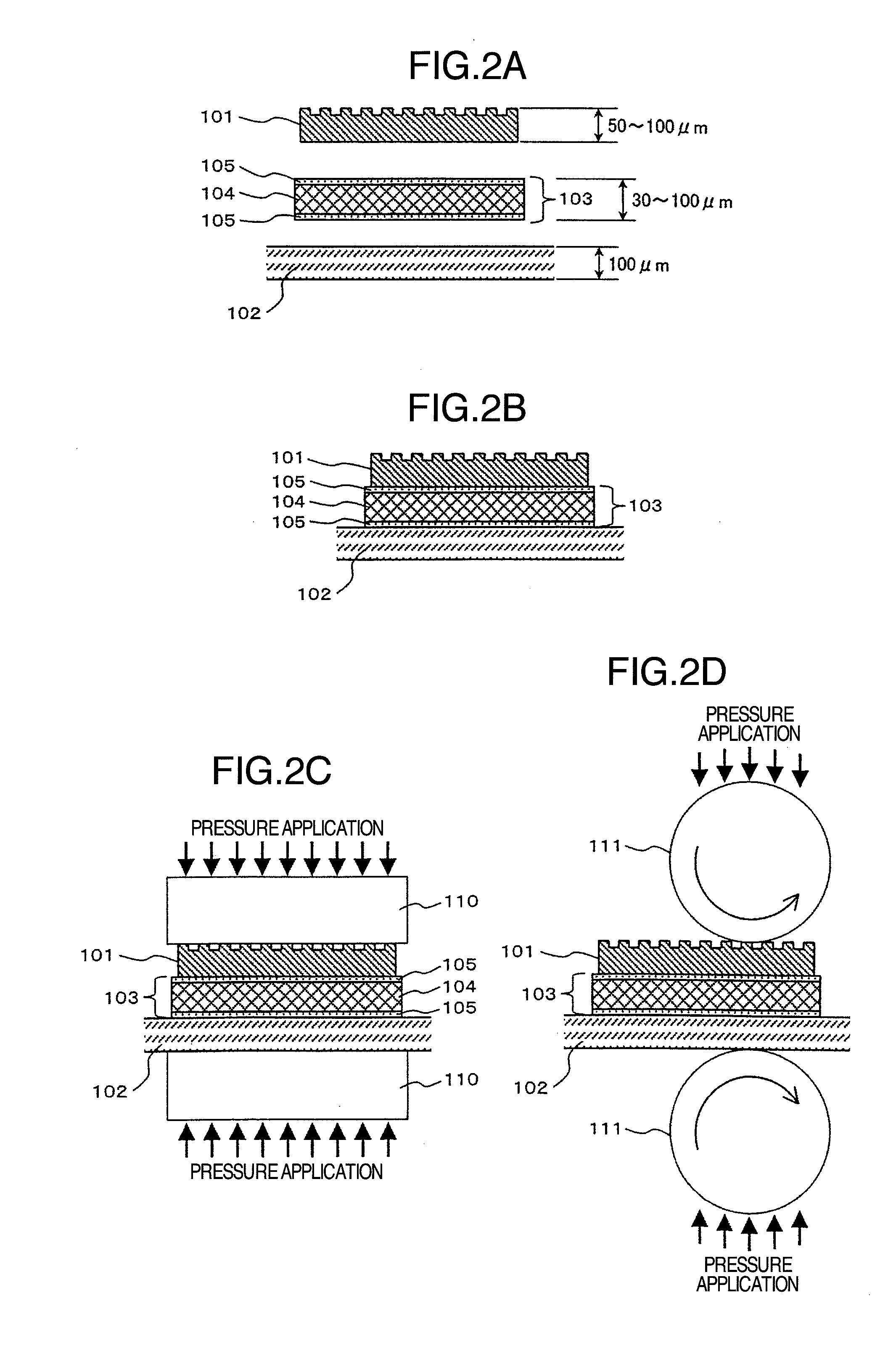
[0059]FIGS. 1A to 1C are schematic diagrams illustrating a belt-shaped mold according to a first embodiment of the present invention. Specifically, FIG. 1A is an overall perspective of a belt-shaped mold 100, FIG. 1B is a schematic cross-sectional view of the structure of the belt-shaped mold 100, and FIG. 1C is a schematic cross-sectional view of an adhesive member. For the belt-shaped mold 100, a plurality of stampers 100 having fine, convex-and-concave patterns are arranged along one surface of an endless belt 102. As shown in FIG. 1B, an adhesive member 103 is provided by depositing a layer, made of a thermosetting resin 105, on the obverse and reverse sides of a porous member 104, and is located between the stampers 101 and the endless belt 102. The stampers 101 and the endless belt 102 are fixed by being adhered to the thermosetting resin 105 layers on the obverse and reverse of the adhesive member 103. As shown in FIG. 1C, pores are contiguously formed inside the porous membe...

embodiment 2

[0067]According to a second embodiment of the present invention, the structure of an adhesive member 103 used for a belt-shaped mold 100 will be described in more detail. In the first embodiment, a description has been given on the assumption that the faces of the stampers 101 and the face of the endless belt 102 to be adhered to the adhesive member 103 are sufficiently smooth. However, when the faces of the stampers 101 and the endless belt 102 to adhere to the adhesive member 103 are rough (the surfaces are too uneven to ignore), an unexpected delamination phenomenon may occur due to insufficient adhesiveness with the adhesive member 103.

[0068]The cause of the delamination phenomenon is considered as follows. FIGS. 4A to 4C are schematic cross-sectional views for explaining the cause of the delamination phenomenon that occurs during the manufacture of the belt-shaped mold 100. In the structure illustrated in FIG. 4A, a thermosetting resin 105 is deposited that has the same thickne...

embodiment 3

[0071]For a third embodiment of the present invention, a relationship is required between the sizes of an adhesive member 103 and each stamper 101 of a belt-shaped mold 100. FIGS. 6A and 6B are schematic cross-sectional views for explaining another structural factor applicable to the adhesive member 103 in the structure of the belt-shaped mold 100 of this embodiment. The structure in FIG. 6A is for a thermal bonding time in a case wherein the adhering face of the stamper 101 is the same size as is the adhesive member 103, and the structure in FIG. 6B is for a thermal bonding time in a case wherein the adhering face of the adhesive member 103 is larger than is the stamper 101. It should be noted that “size” represents the size of a projection face, and more specifically, represents the length, in the circumferential direction, of the endless belt 102 and the length in the direction of the width.

[0072]When a thermal bonding process was performed for the structures in FIGS. 6A and 6B, ...


PUM

PropertyMeasurementUnit
heightaaaaaaaaaa
widthaaaaaaaaaa
aspect ratioaaaaaaaaaa

Abstract

There is provided a fine pattern transfer, belt-shaped mold, with which a fine structure having a high aspect ratio can be formed rapidly and stably using nanoimprinting, and a fine pattern transfer system (a nanoimprint system) that employs this mold. According to the present invention, a nanoimprint mold includes: a belt-shaped support member; a plurality of stampers, for each of which a fine convex-and-concave pattern, to be transferred, is formed on one surface; and an adhesive member, to which the belt-shaped support member and the stampers are to be securely adhered, wherein the adhesive member includes a porous member and adhesive layers, which are deposited on either face of the porous member, for impregnating one part of the porous member, and wherein, for the porous member, a porous area that is not impregnated with the adhesive layers, is provided and positioned so as to sandwich the porous member between portions impregnated with the adhesive layers.

Description

BACKGROUND OF THE INVENTION[0001](1) Field of the Invention[0002]The present invention relates to a pattern transfer mold and to a transfer system for employing the pattern transfer mold, and relates particularly to a fine structure transfer mold, with which the nanoimprinting transfer of a fine pattern can be performed very accurately, at a low cost, and a fine structure transfer system for employing this mold.[0003](2) Description of Related Art[0004]Conventionally, photolithography technology is employed for processing fine patterns required for semiconductor integrated circuits. However, in consonance with developments in the structural refinement and the integration of circuits, required element sizes have been reduced until they are the equivalent of the wavelengths of light sources used for photolithography exposure, and fabricating such fine patterns using photolithography is difficult. Therefore, instead of a system that employs photolithography, one that uses electron beam...

Claims


Application Information

Patent Timeline
Patent Type & Authority Applications(United States)
IPC IPC(8): B29C33/36
CPCB29C59/04B29C2059/023G03F7/0002B82Y40/00B82Y10/00Y10S977/887
Inventor HASEGAWA, MITSURUOGINO, MASAHIKO
Owner HITACHI LTD
Why Eureka
Try Eureka