Semiconductor storage device

a technology of semiconductors and storage devices, applied in the direction of instruments, coding, code conversion, etc., can solve the problems of increasing process time, increasing wiring length, increasing layout area, etc., and achieves the effect of reducing chip area, yield and reliability, and improving ecc process performan

Active Publication Date: 2009-04-02
PANASONIC SEMICON SOLUTIONS CO LTD
View PDF14 Cites 53 Cited by
  • Summary
  • Abstract
  • Description
  • Claims
  • Application Information

AI Technical Summary

Benefits of technology

[0044]The present invention is a technique that is applicable and effective to a semiconductor storage device with an ECC function, particularly one that has a multi-bit data configuration. The ECC process performance can be improved while suppressing a

Problems solved by technology

According to U.S. Pat. No. 5,384,789, the syndrome generating circuit, the syndrome decoding circuit, and the error correcting circuit are provided in common to each block and are arranged at separate positions, so that if the bit width of the ECC process increases, the wiring region increases, leading to an increase in layout area, and also, the wiring length increases, leading to an increase in process time.
Conversely, when the bit width of the ECC process increases, the proportion of check bits decreases, but the number of wiring lines between a memory array and an ECC process circuit increases, leading to an increase in chip area.
Further, the wiring line between the memory array and

Method used


Image

  • Semiconductor storage device
  • Semiconductor storage device
  • Semiconductor storage device

Examples


embodiment 1

Variation 4 of Embodiment 1

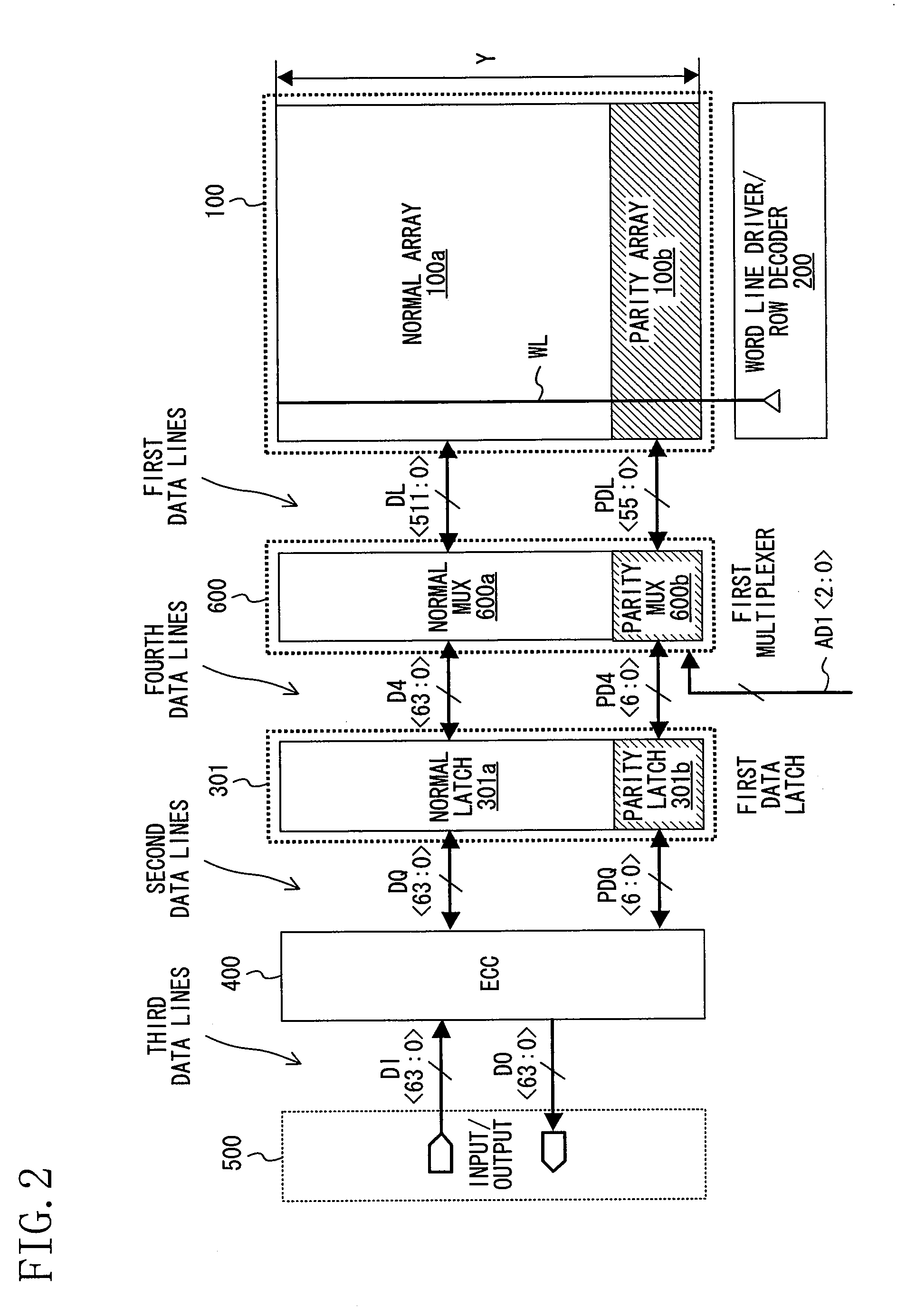
[0097]FIG. 5 is a diagram schematically showing a configuration of a semiconductor storage device with an ECC circuit according to Variation 4 of Embodiment 1 of the present invention. Variation 4 is different from Embodiment 1 (see FIG. 1) in that a multiplexer is provided before and after an ECC circuit section 401, and the number of ECC process bits is 128 bits.

[0098]In this embodiment, second data lines latched by the first data latch column 300 are input via a first multiplexer column 601 to the ECC circuit section 401. Fifth data lines that have been subjected to error correction by the ECC circuit section 401 are input via a second multiplexer column 602 to an input / output circuit section 500.

[0099]The first multiplexer column 601 includes 128 second normal multiplexers 601a and 8 second parity multiplexers 601b, and for example, has a 4-to-1 selection function in accordance with a 2-bit address signal AD1. For example, a fourth normal data line D4 ...

embodiment 2

Variation 3 of Embodiment 2

[0146]FIG. 16 is a schematic diagram showing a power supply wiring configuration in a semiconductor storage device according to Variation 3 of Embodiment 2. In FIG. 16, word line shunt wiring lines UWL , a data latch control signal EN, address signals AD for controlling selection of a multiplexer, and syndrome signals SYND are formed in a first wiring layer in a direction parallel to the word line shunt wiring lines UWL . First data lines DL and NDL , a read data line RD , and a write data line WD are formed in a second wiring layer in a direction orthogonal to the word line shunt wiring lines UWL .

[0147]A power supply line VDD and a ground line VSS are formed in parallel in the same wiring layer as the first wiring layer, and a power supply line VDD and a ground line VSS are formed in parallel in the same wiring layer as the second wiring layer. The power supply lines VDD and the ground lines VSS in the first wiring layer and the second wiring layer a...

embodiment 3

[0150]FIG. 17 is a block diagram showing a configuration of a memory array and an ECC circuit section in a semiconductor storage device according to Embodiment 3 of the present invention. As compared to Variation 4 of Embodiment 1 (see FIG. 5), four memory blocks 10 each including the circuit sections except for the word line driver / row decoder 200 are configured and provided. The memory blocks 10 perform data read and write operations using word lines WL with the same access cycle and the same address.

[0151]As in this embodiment, a word line driver / row decoder 200 is provided in common to the memory blocks 10. The memory blocks 10 are successively arranged so that the word lines WL extending in a straight line can be connected in common thereto. Thereby, the chip area can be reduced. Further, the memory blocks 10 can be simultaneously operated in parallel, so that the number of data bits in the whole device can be easily increased without increasing the number of process bits per...


PUM


Abstract

Data latches, multiplexers, an ECC circuit section, and an input/output circuit section are arranged in columns and adjacent to each other, in an extending direction of data lines that are formed in a direction orthogonal to word lines. A layout of a data path system is formed in bit slices. Further, parity bits are equally distributed so as to cause delay times of bits to be uniform.

Description

BACKGROUND OF THE INVENTION[0001]1. Field of the Invention[0002]The present invention relates to a semiconductor storage device, and more particularly, to a semiconductor storage device comprising an Error Checking and Correcting (ECC) circuit.[0003]2. Description of the Related Art[0004]In recent years, as semiconductor manufacturing techniques have been advanced, devices have been increasingly miniaturized. For example, the packaging density of a semiconductor storage device, such as representatively a dynamic random access memory (hereinafter referred to as a DRAM) or a static random access memory (hereinafter referred to as an SRAM), has been improved.[0005]A redundant relief technique is generally known in which a defective memory cell is replaced with a spare memory cell in order to improve the yield of a DRAM or an SRAM. However, the redundant relief technique cannot overcome a defect occurring due to a deterioration in characteristics of an element during use or a defect occ...

Claims


Application Information

Patent Timeline
IPC IPC(8): G11C29/52G06F11/10
CPCG06F11/1048G11C5/025G11C7/1006G11C2029/0411G11C7/1051G11C7/106G11C29/70G11C7/1012
Inventor HIROSE, MASANOBUIIDA, MASAHISA
Owner PANASONIC SEMICON SOLUTIONS CO LTD
Why Eureka
Try Eureka