System and method for plasma enhanced thin film deposition

a plasma enhanced and thin film technology, applied in the field of system and a method for plasma enhanced thin film deposition, can solve the problems of complex processing, low throughput, and low crystallinity, and achieve the effect of high deposition ra

Inactive Publication Date: 2009-04-09
IND TECH RES INST
View PDF4 Cites 15 Cited by
  • Summary
  • Abstract
  • Description
  • Claims
  • Application Information

AI Technical Summary

Benefits of technology

[0008]It is an object of the present invention to provide to a system and a method for plasma enhanced thin film deposition, capable of providing real-time monitoring and analysis on the radical spectrum for calculation on spectrum intensity ratio to modulate the pulse power parameters to obtain a high-quality microcrystalline silicon thin film by preventing amorphous silicon from growing at a high deposition rate.
[0023]It is preferable that the pulsed plasma modulation device shortens the pulsed plasma duty time to avoid the formation of amorphous silicon if the spectrum intensity ratio r is larger than the crystallization transition value R, otherwise the pulsed plasma modulation device lengthens the pulsed plasma duty time to achieve high deposition rate if the spectrum intensity ratio r is smaller than the crystallization transition value R.

Problems solved by technology

Conventionally, the microcrystalline silicon thin film is grown by plasma enhanced chemical vapor deposition (PECVD) with low deposition rate and non-uniform crystallinity, which results in issues such as low throughput and low crystallinity.
However, JP 20030421313 does not provide real-time monitoring and quantitative analysis for the ionized gas during thin film deposition.
In FIG. 1, only two steps of process time T and pulsed plasma duty time ratio Pr are shown; however, in practical cases, the pulsed plasma duty time ratio Pr is required to be divided into multiple steps with pre-determined conditions for multi-step processing to achieve optimal deposition rate, which leads to complicated processing.
Moreover, JP 20030421313 discloses an open-loop system, in which the ionization rate of the reactive gas is unstable due to gas flow and deposition on electrodes during long thin film deposition time in a mass-production manner, which affects the effects of pre-determined conditions and results in thin film quality not as good as expected.

Method used


Image

  • System and method for plasma enhanced thin film deposition
  • System and method for plasma enhanced thin film deposition
  • System and method for plasma enhanced thin film deposition

Examples


Embodiment Construction

[0039]The present invention can be exemplified but not limited by the preferred embodiment as described hereinafter.

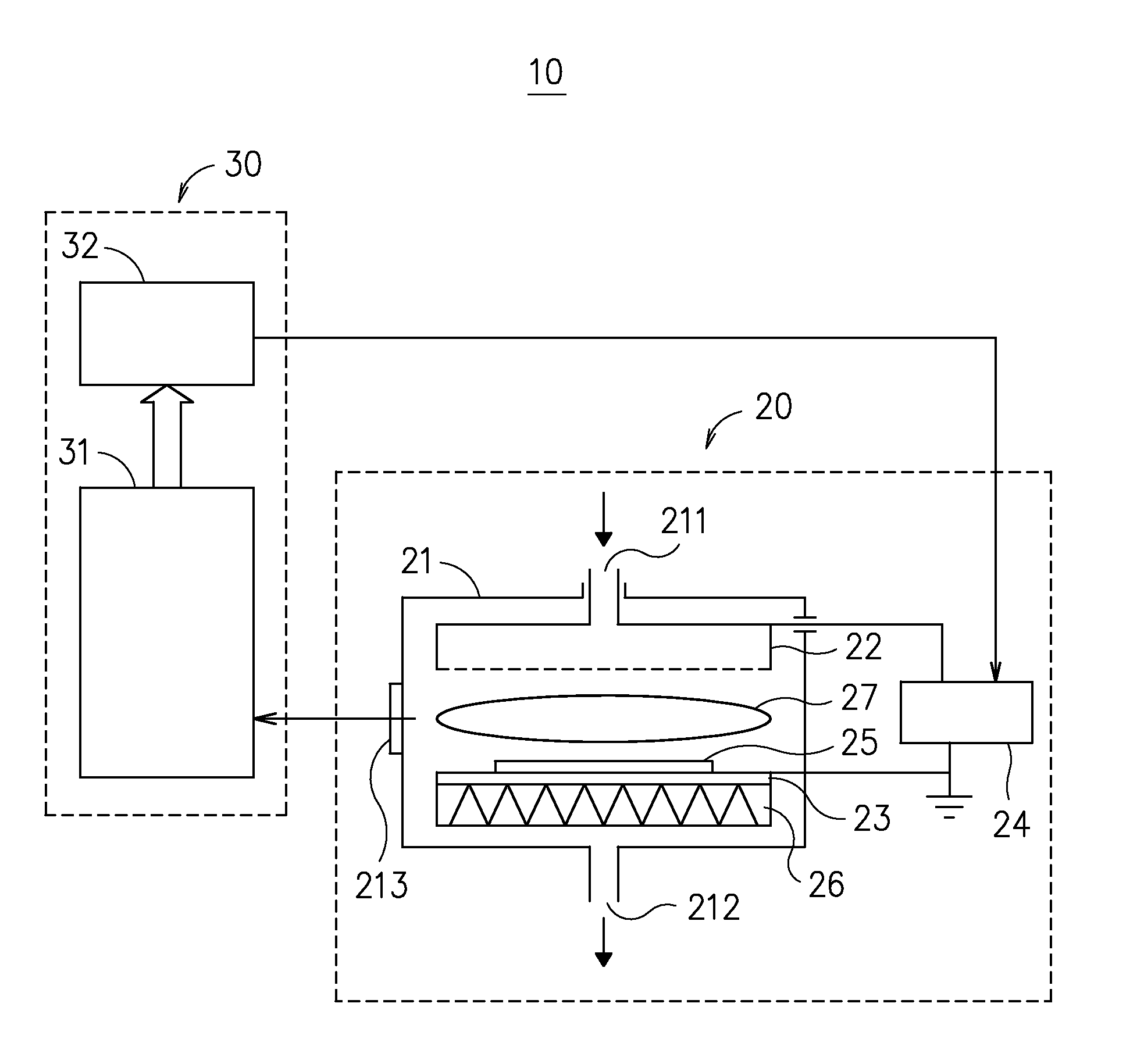
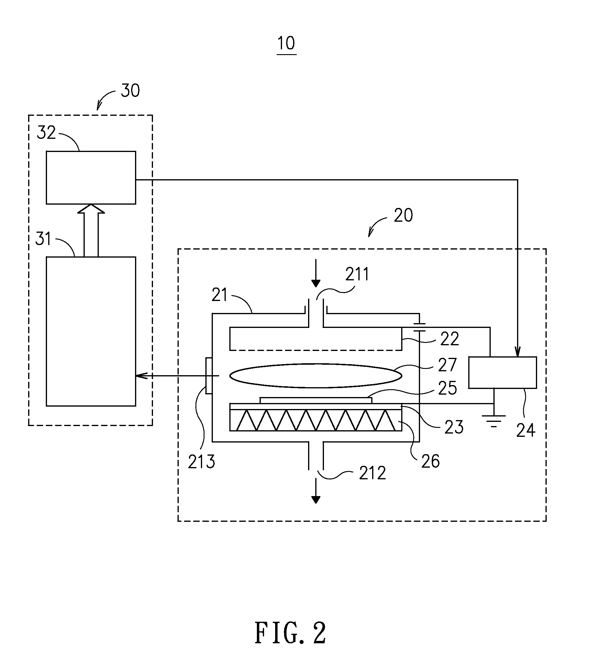
[0040]Please refer toFIG. 2, which is schematic diagram showing a system for plasma enhanced thin film deposition according to the present invention. The plasma enhanced thin film deposition system 10 comprises a plasma enhanced thin film deposition apparatus 20 and a plasma process monitoring device 30.

[0041]In FIG. 2, the plasma enhanced thin film deposition apparatus 20 is a plasma enhanced chemical vapor-phase deposition (PECVD) apparatus, comprising: a chamber 21, having a reactive gas inlet 211 and a gas outlet 212. Inside the chamber 21, there is installed a top electrode 22 and a bottom electrode 23. The top electrode 22 is coupled to one terminal of a pulsed power supply 24. The bottom electrode 23 is capable of carrying a substrate 25 whereon a thin film deposits so that the substrate 25 is interposed between the top electrode 22 and the bottom electrode 23. ...


PUM

PropertyMeasurementUnit
thicknessaaaaaaaaaa
optical emission spectroscopyaaaaaaaaaa
spectrum intensitiesaaaaaaaaaa

Abstract

A system and a method for plasma enhanced thin film deposition are disclosed, in which the system comprises a plasma enhanced thin film deposition apparatus and a plasma process monitoring device. The plasma enhanced thin film deposition apparatus receives pulsed power and a reactive gas, whereby plasma discharging occurs to ionize the reactive gas into a plurality of radicals for thin film deposition. The plasma process monitoring device comprises an optical emission spectroscopy (OES) and a pulsed plasma modulation device, in which the OES detects spectrum intensities of the radicals and the pulsed plasma modulation device calculates a spectrum intensity ratio of the radicals so as to modulate the plasma duty time of pulsed power, thereby high deposition rate as well as real-time monitoring on thin film deposition quality can be achieved.

Description

BACKGROUND OF THE INVENTION[0001]1. Field of the Invention[0002]The present invention generally relates to a system and a method for plasma enhanced thin film deposition and, more particularly, to a system and a method for plasma enhanced thin film deposition, using an optical emission spectroscopy (OES) detecting spectrum intensities of the radicals and a pulsed plasma modulation device calculating a spectrum intensity ratio of the radicals so as to modulate pulsed plasma parameters, thereby high deposition rate as well as real-time monitoring on thin film deposition quality can be achieved.[0003]2. Description of the Prior Art[0004]The microcrystalline silicon (μc-Si) thin film is used in tandem Si-based thin film solar cells with high photoelectric conversion efficiency. Conventionally, the microcrystalline silicon thin film is grown by plasma enhanced chemical vapor deposition (PECVD) with low deposition rate and non-uniform crystallinity, which results in issues such as low thr...

Claims


Application Information

Patent Timeline
Patent Type & Authority Applications(United States)
IPC IPC(8): C23C14/32
CPCC23C16/24C23C16/52C23C16/50
Inventor DU, CHEN-CHUNGHUANG, JEN-RONGLIANG, MUH-WANGCHANG, CHIH-CHENLEE, SHENG-LANGWU, CHING-HUEILO, CHAN-HSING
Owner IND TECH RES INST
Why Eureka
Try Eureka