Spatial Light Modulators and Fabrication Techniques

a technology of spatial light modulator and fabrication technique, which is applied in the direction of lamination ancillary operations, instruments, chemistry apparatus and processes, etc., can solve the problems of high cost of packaging die-level devices and tolerating raised temperatures, and achieve low cost, cost saving, and reduced device fabrication costs.

Inactive Publication Date: 2012-07-05
LIGHT BLUE OPTICS
View PDF3 Cites 2 Cited by
  • Summary
  • Abstract
  • Description
  • Claims
  • Application Information

AI Technical Summary

Benefits of technology

[0009]Employing wafer-level processing for packaging reduces the device fabrication cost. In embodiments the upper, glass wafer may optionally be diced partially or wholly through the bond lines.
[0010]In embodiments of the method a significant further advantage is provided by selectively removing a portion of the glass wafer adjacent each device to reveal at least some of the electrical connectio...

Problems solved by technology

One problem with the fabrication of an optical MEMS SLM is that packaging the die-level device is expensive.
A further problem is that a very thin seal between the MEMS substrate and the overlaying glass window is desirable, to minimise water ingress, reduce outgassing from the adhesive, and provide good adhesion and good hermetic sealing.
One approach is to deposit an epoxy-based adhesive from a syringe onto the MEMS substrate, but this is expens...

Method used


Image

  • Spatial Light Modulators and Fabrication Techniques
  • Spatial Light Modulators and Fabrication Techniques
  • Spatial Light Modulators and Fabrication Techniques

Examples


Embodiment Construction

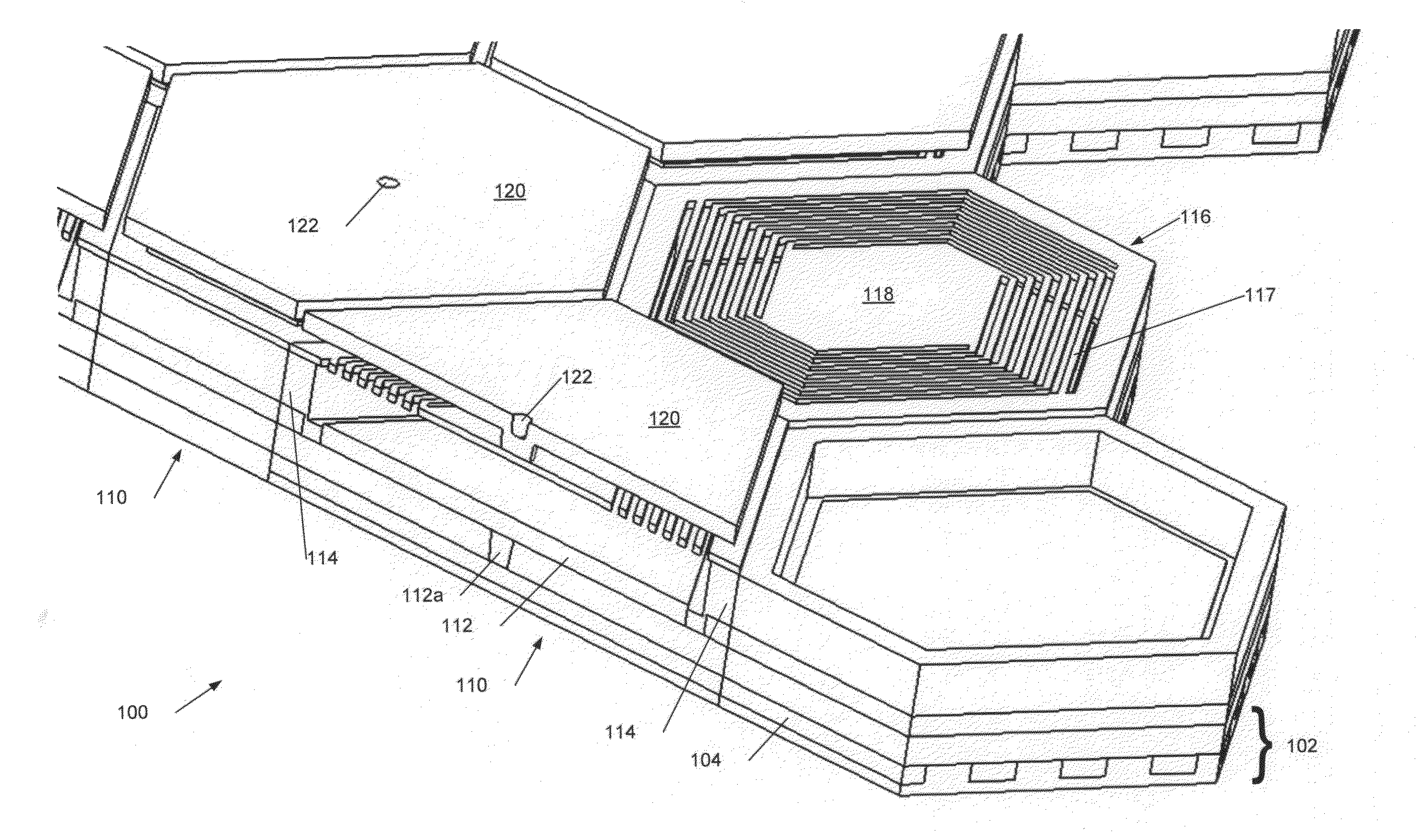
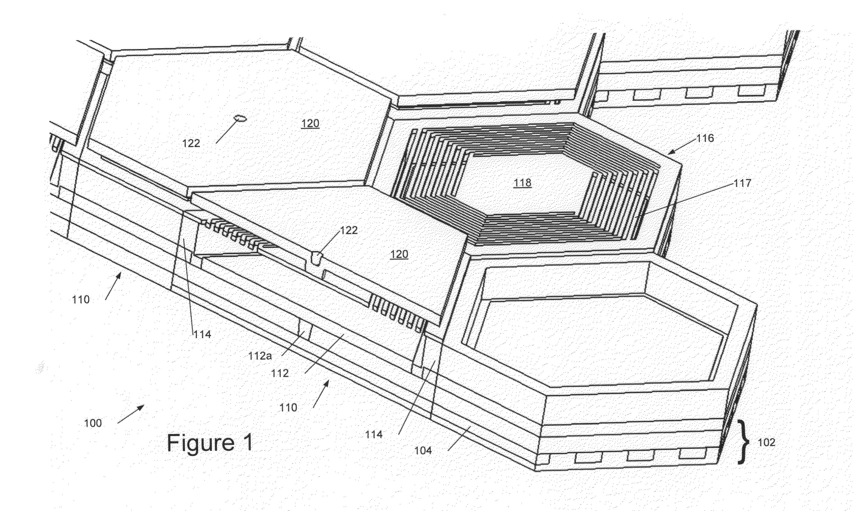
[0028]Referring first to FIG. 1, this shows a cutaway portion of an optical phase modulating MEMS SLM 100 prior to attaching a glass window over the MEMS pixels.

[0029]In the example of FIG. 12 each electrostatically-actuated pixel is approximately 10×10√{square root over (2)} μm and deflects over 400 nm when actuated with 1 volts, has 8 nm of deflection resolution, settles within 30 μs, and has the shape of an irregular hexagon. The mirror spring comprises a single crystal silicon (SCS) electromechanical flexure serving as both a spring / mirror mount and as a top electrode.

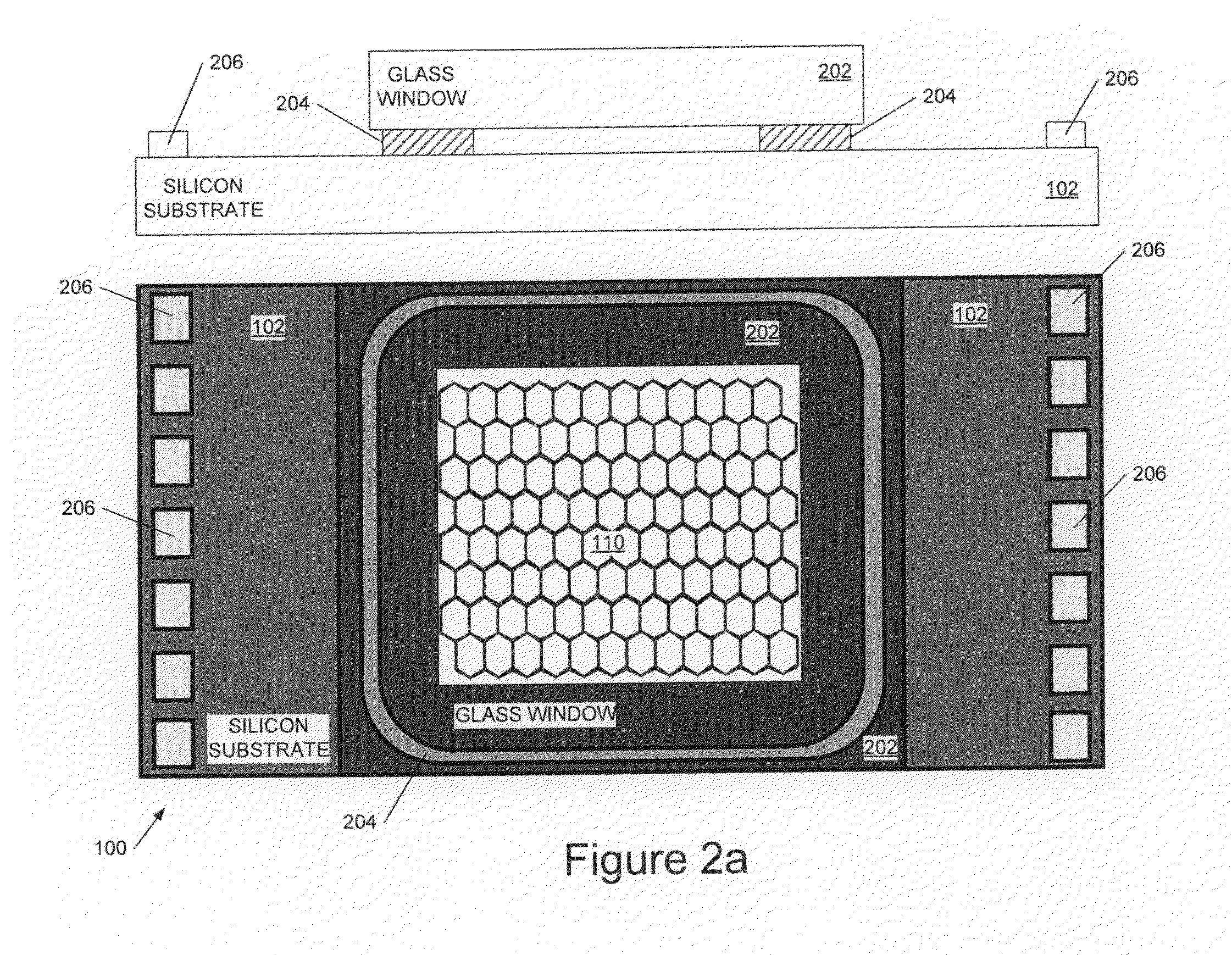
[0030]Thus in some preferred embodiments the SLM 100 comprises a substrate 102 bearing a plurality of SLM pixels 110. For display devices, individual addressing of mirror actuators is generally desirable, and this may be achieved by incorporating CMOS circuitry underneath each actuator. Thus substrate 102 is preferably a CMOS substrate and a bottom pixel electrode 112 may comprise a portion of an exposed top metal ...


PUM

PropertyMeasurementUnit
Temperatureaaaaaaaaaa
Pressureaaaaaaaaaa

Abstract

We describe a method of fabricating an optical MEMS spatial light modulator (SLM). The method comprises providing an optical MEMS SLM wafer bearing multiple optical MEMS SLM devices and spin coating a glass wafer with an organic adhesive, in some preferred embodiments benzocyclobutene. The adhesive is patterned, preferably by uv lithography, to define multiple ring-shaped bond lines each sized to fit around one of the SLM devices, and the glass wafer is then bonded to the MEMS SLM wafer, preferably at a temperature of between 100° C. and 450° C., such that each of the ring-shaped bond lines encompasses a respective SLM device. A portion of the glass wafer adjacent an SLM device is then removed to reveal electrical connectors to the device and the devices are tested before dicing and packaging, to enable selective packaging of working devices.

Description

COPYRIGHT NOTICE[0001]Contained herein is material that is subject to copyright protection. The copyright owner has no objection to the facsimile reproduction of the patent disclosure by any person as it appears in the Patent and Trademark Office patent files or records, but otherwise reserves all rights to the copyright whatsoever. Copyright © 2010, Light Blue Optics Inc.BACKGROUND[0002]1. Field[0003]Embodiments of the present invention generally relate to techniques for fabricating / packaging spatial light modulators (SLMs), in particular optical MEMS (micro electro mechanical system)—based piston-type phase modulating devices, and to spatial light modulators fabricated / packaged using such techniques.[0004]2. Description of the Related Art[0005]We have previously described various holographic image projection systems (see, for example, WO2010 / 007404 and U.S. Ser. No. 12 / 182,095) and, more particularly, an analogue optical phase modulating MEMS SLM for use in such systems, in embodi...

Claims


Application Information

Patent Timeline
IPC IPC(8): G02B26/00B32B38/04
CPCY10T156/1052G02B26/0841
Inventor GUPTA, PAVANMATUS, GABRIELNOVOTNY, VLAD
Owner LIGHT BLUE OPTICS
Why Eureka
Try Eureka