Charged particle application apparatus

a technology of application apparatus and charged particles, which is applied in the direction of material analysis using wave/particle radiation, instruments, nuclear engineering, etc., can solve the problems that the detection function of the detector cannot be exercised simultaneously with the measurement function of the probe light, and cannot be installed under an objective lens or in a limited spa

Inactive Publication Date: 2009-04-23
HITACHI HIGH-TECH CORP
View PDF8 Cites 41 Cited by
  • Summary
  • Abstract
  • Description
  • Claims
  • Application Information

AI Technical Summary

Problems solved by technology

Therefore, such detectors cannot be installed under an objective lens or in a limited space.
Furthermore, the detectors based on the conventional technologies are sensitive to light so that their detection function cannot be exercised simultaneously with the measurement function of probe light.

Method used


Image

  • Charged particle application apparatus
  • Charged particle application apparatus
  • Charged particle application apparatus

Examples


first embodiment

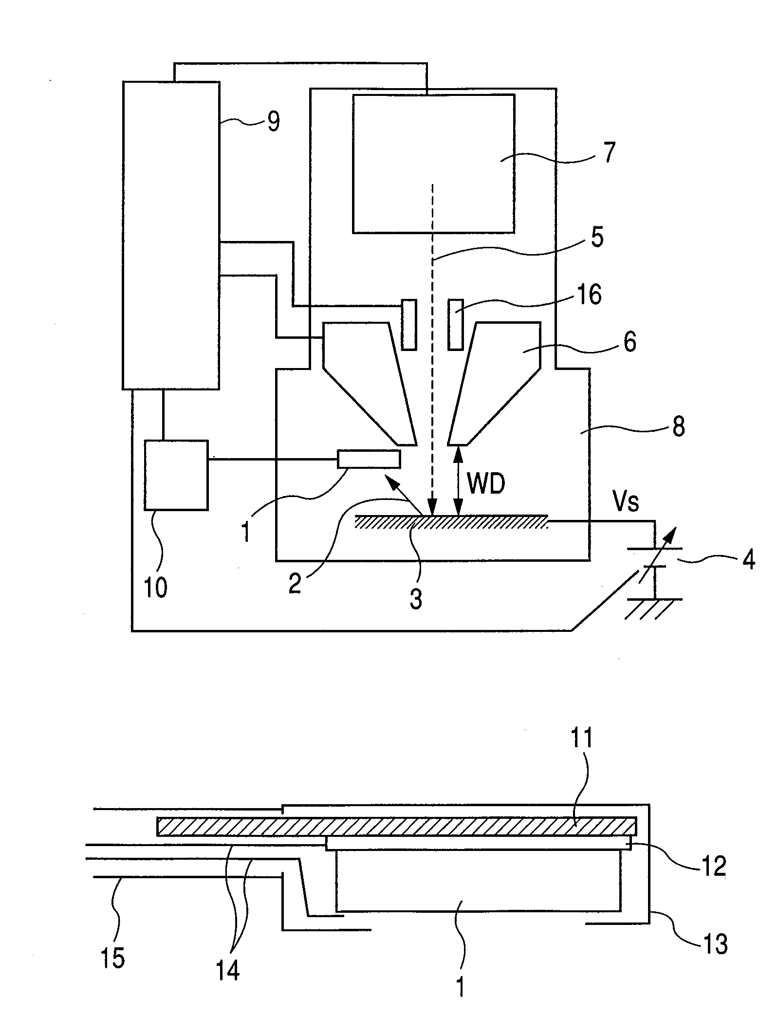
[0038]FIGS. 1(a) to 1(c) show a charged particle beam application apparatus according to a first embodiment of the present invention.

[0039]The present invention can be applied not only to a scanning electron microscope (SEM) but also to a charged particle beam application apparatus including, for instance, a microscope based on an ion beam.

[0040]The description of the present embodiment relates to an electron detector (electron detection section) that is thin and highly sensitive to low energy electrons, and to a case where the electron detector is applied to a scanning electron microscope as an example of the charged particle beam application apparatus.

[0041]In a scanning electron microscope, a probe electron beam 5, which is generated from an electron beam irradiation source 7 containing an electron source, is scanned in x-y direction by a deflector 16. Electrons 2, which are secondarily generated from a sample 3, are detected by an electron detector 1, and converted and adjusted ...

second embodiment

[0060]FIGS. 6(a) to 6(e) show the electron detector according to a second embodiment of the present invention, which is configured by using a substrate having a large energy gap.

[0061]The second embodiment will be described on the assumption that a diamond substrate is used as the substrate having a large energy gap. In the present embodiment, comb-like electrodes 101, 102 are mounted on a surface of the diamond substrate and positioned face to face. When electrons are injected while a potential difference of 10 to 100 V is applied across the electrodes, the incident electrodes generate electron-hole pairs. The electrons travel toward the positive (+) electrode, whereas the holes travel toward the negative (−) electrode.

[0062]Since the hole ionization rate is high within diamond, avalanche multiplication is solely determined by the holes traveling in a high electric field. FIG. 8 is a schematic structural cross-sectional view of avalanche multiplication. When an electron beam is to ...

third embodiment

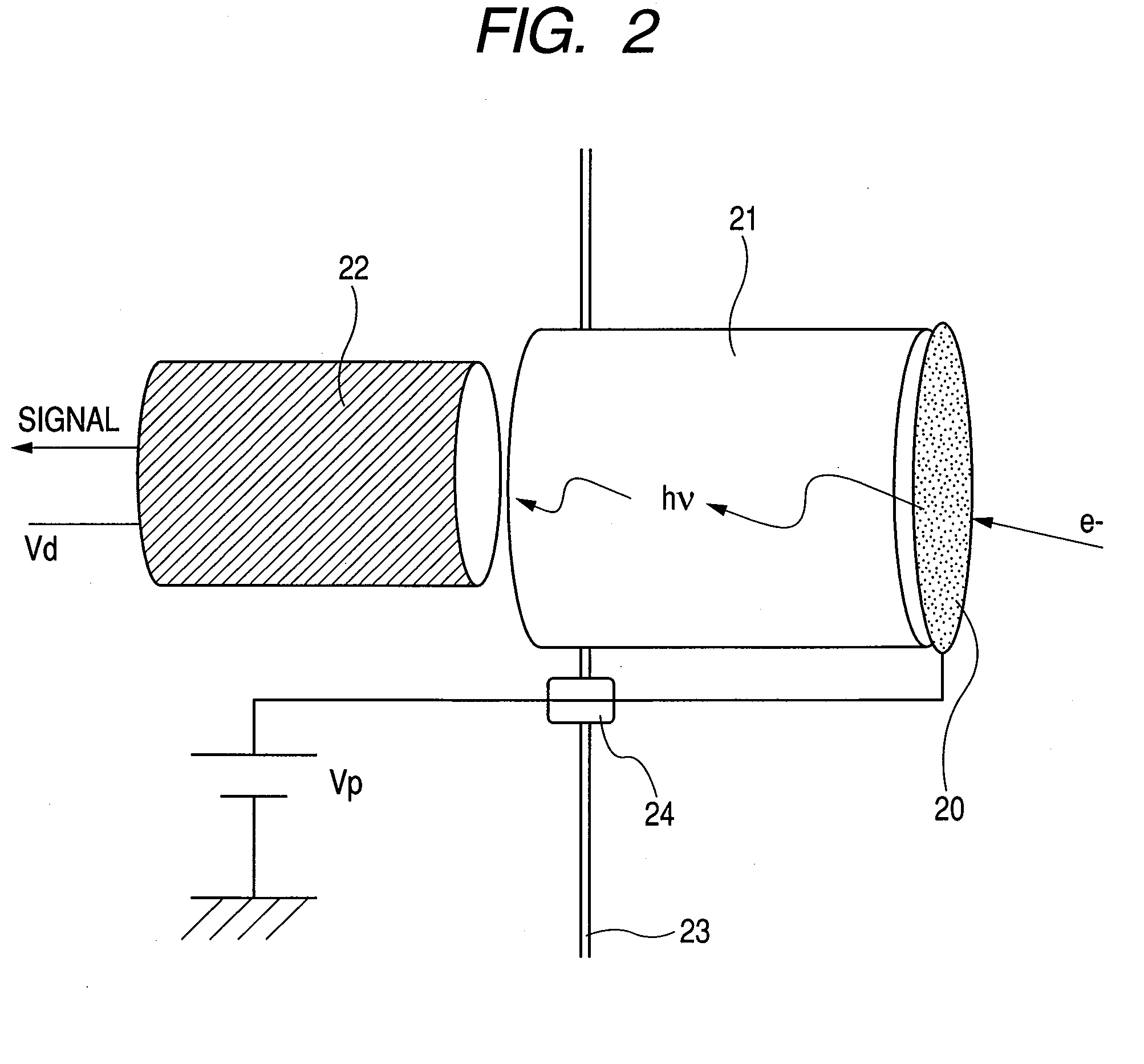
[0071]FIG. 9 is a conceptual diagram illustrating a typical electron beam apparatus that makes use of compactness and high sensitivity of the detector according to the present invention. FIG. 9 shows a scanning electron microscope (SEM) as an example of the electron beam apparatus. Probe electrons 5 generated from the electron beam irradiation source 7 are adjusted so that three electron lenses (L1, L2, and L3 in FIG. 9) form a very small focus spot on the surface of the sample 3. The deflector then sweeps the focus spot in x and y directions. Electrons generated from the sample are converted to an electrical signal by the detector so as to observe a microscopic region of the sample surface. Although the deflector is not shown in the figure, it is positioned between lenses L1 and L2. A substrate bias voltage source 4 applies a voltage Vs to the sample 3. The employed structure is configured to decelerate the probe electrons 5 immediately before the sample 3 so that high-resolution o...


PUM

PropertyMeasurementUnit
energyaaaaaaaaaa
acceleration voltageaaaaaaaaaa
thicknessaaaaaaaaaa

Abstract

The present invention provides a highly sensitive, thin detector useful for observing low-voltage, high-resolution SEM images, and provides a charged particle beam application apparatus based on such a detector. The charged particle beam application apparatus includes a charged particle irradiation source, a charged particle optics for irradiating a sample with a charged particle beam emitted from the charged particle irradiation source, and an electron detection section for detecting electrons that are secondarily generated from the sample. The electron detection section includes a diode device that is a combination of a phosphor layer, which converts the electrons to an optical signal, and a device for converting the optical signal to electrons and subjecting the electrons to avalanche multiplication, or includes a diode device having an electron absorption region that is composed of at least a wide-gap semiconductor substrate with a bandgap greater than 2 eV.

Description

CLAIM OF PRIORITY[0001]The present application claims priority from Japanese patent application JP 2007-271609, filed on Oct. 18, 2007, the content of which is hereby incorporated by reference into this application.BACKGROUND OF THE INVENTION[0002]The present invention relates to a charged particle application apparatus that contains a scanning electron microscope (SEM) for observing a microstructure with an electron beam.[0003]Conventional scanning electron microscopes (SEMs) mostly use an E-T (Everhart-Thornley) detector for low energy secondary electrons as an electron beam detector for microscope image acquisition. As shown in FIG. 2, the E-T detector causes electrons (e−) generated from a sample to collide against a scintillator 20 for the purpose of generating light (hν), allows a light guide 21 to move the generated light (hν) outside a wall 23 of a vacuum device, and permits a photomultiplier 22 to detect the light (hν) and generate a signal current. In FIG. 2, Vp is a volta...

Claims


Application Information

Patent Timeline
Patent Type & Authority Applications(United States)
IPC IPC(8): G01N23/00
CPCH01J37/244H01J37/28H01J37/3056H01J2237/2482H01J2237/2443H01J2237/2444H01J2237/2445H01J2237/2441
Inventor OHSHIMA, TAKASHIHATANO, MICHIONAGAISHI, HIDEYUKISATO, MITSUGUFUKUDA, MUNEYUKI
Owner HITACHI HIGH-TECH CORP
Why Eureka
Try Eureka