Surface emitting laser and manufacturing method thereof
- Summary
- Abstract
- Description
- Claims
- Application Information
AI Technical Summary
Benefits of technology
Problems solved by technology
Method used
Image

Examples
Embodiment Construction
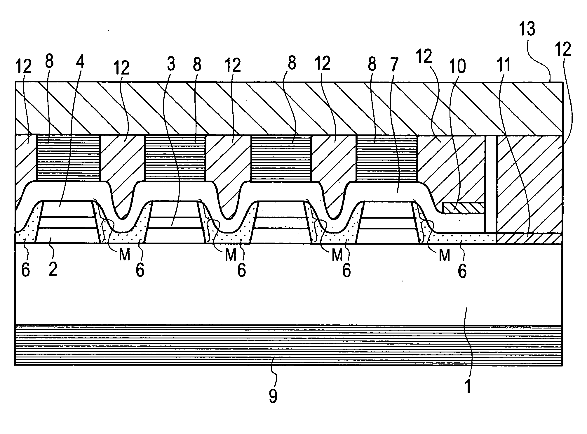
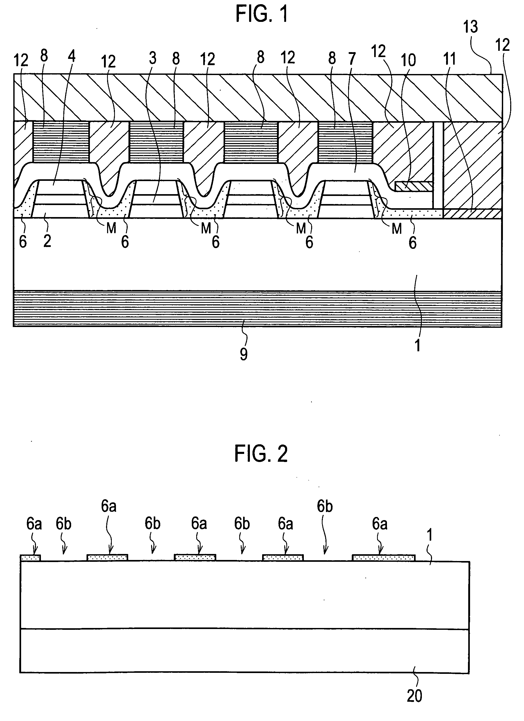
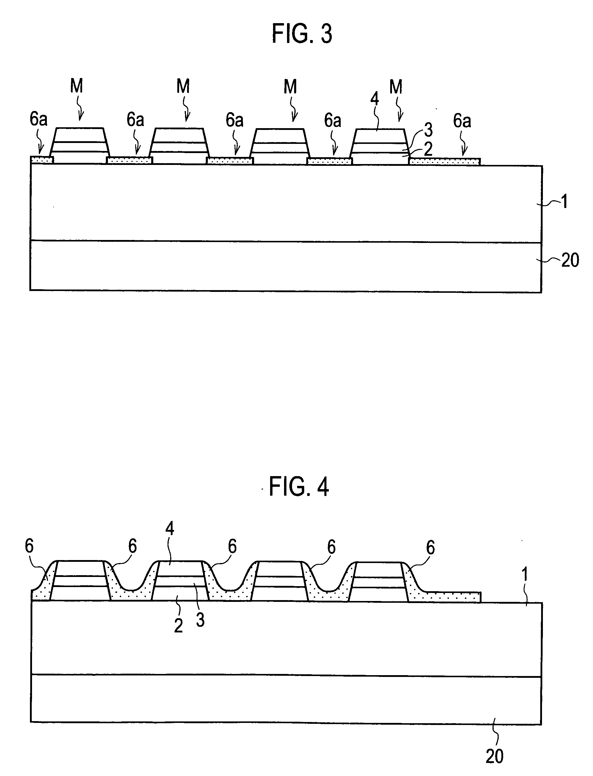
[0039]One embodiment of the present invention will be described below with reference to the drawings. FIG. 1 shows the sectional structure of a surface emitting laser of the present invention.
[0040]The surface emitting laser is formed of a nitride semiconductor. With an n-type GaN buffer layer 1 as a common semiconductor layer, a plurality of mesa regions M are formed on the GaN buffer layer 1 in one-dimensional array or two-dimensional array. The mesa region M is formed of a semiconductor layer formed of an n-type GaN layer 2, an active layer 3, and a p-type GaN layer 4. Here, the nitride semiconductor refers to an AlGaInN quaternary mixed crystal and is called a III-V nitride semiconductor, which can be represented by AlxGayInzN (x+y+z=1, 0≦x≦1, 0≦y≦1, 0≦z≦1).
[0041]An insulating film 6 formed of, for example, SiO2 (silicon oxide) or SiN (silicon nitride) is formed on the side surfaces of the mesa regions M and the top surface of the GaN buffer layer 1 so as to fill gaps between th...
PUM
 Abstract
Description
Claims
Application Information
 - Generate Ideas
- Intellectual Property
- Life Sciences
- Materials
- Tech Scout
- Unparalleled Data Quality
- Higher Quality Content
- 60% Fewer Hallucinations
Browse by: Latest US Patents, China's latest patents, Technical Efficacy Thesaurus, Application Domain, Technology Topic, Popular Technical Reports.
© 2025 PatSnap. All rights reserved.Legal|Privacy policy|Modern Slavery Act Transparency Statement|Sitemap|About US| Contact US: help@patsnap.com