

Method for manufacturing display device
a technology of display device and manufacturing method, which is applied in the field of display device, can solve the problems of reducing the number of light-exposure masks whose design and manufacturing cost is high, and achieves the effects of low cost, high reliability, and simplified photolithography process
- Summary
- Abstract
- Description
- Claims
- Application Information
AI Technical Summary
Benefits of technology
Problems solved by technology
Method used
Image

Examples
embodiment mode 1
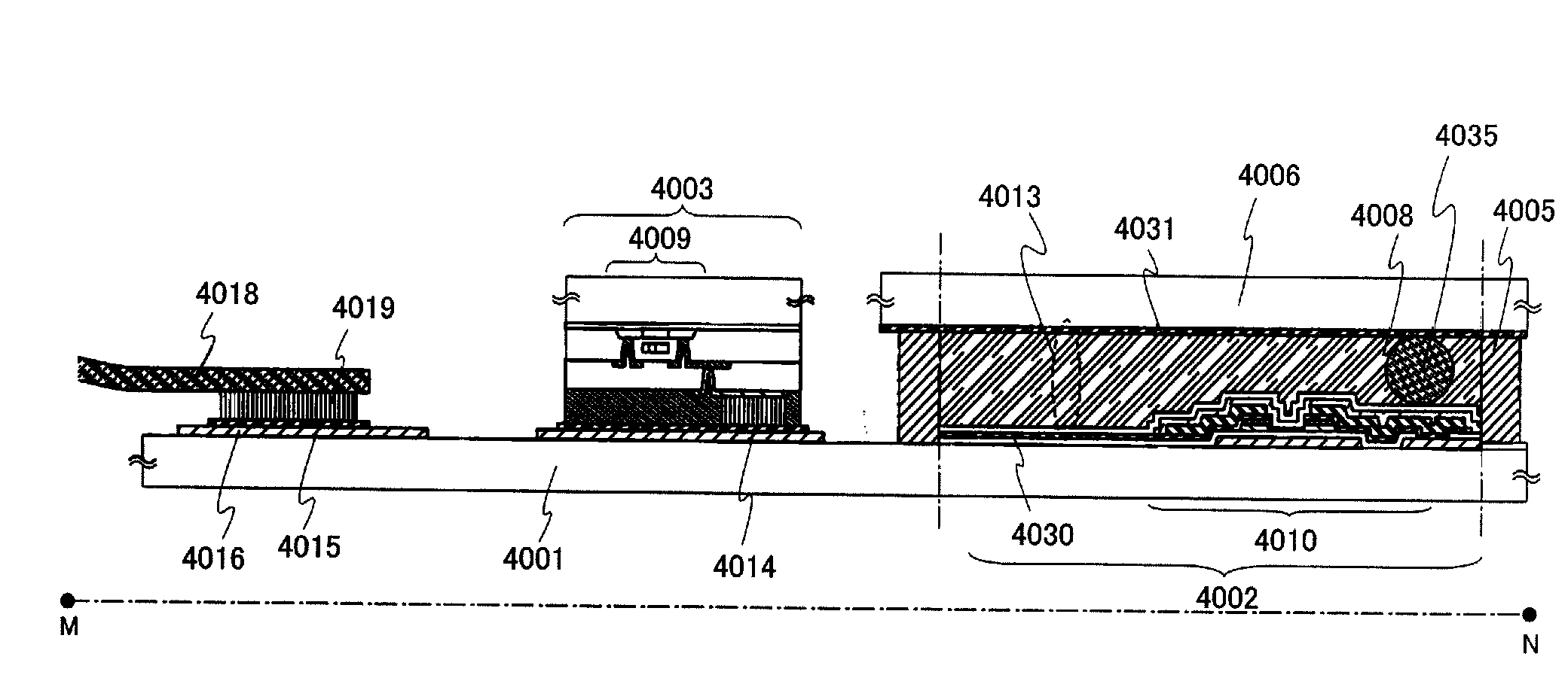
[0033]In this embodiment mode, a display device including a thin film transistor and a manufacturing method thereof will be described with reference to FIGS. 1A to 1C, FIGS. 2A to 2C, FIGS. 3A to 3D, FIGS. 4A to 4D, FIGS. 5A to 5D, FIGS. 6A to 6C, and FIGS. 7A and 7B.
[0034]An n-channel thin film transistor has higher mobility than p-channel thin film transistor. Therefore, an n-channel thin film transistor is more suitable for a driver circuit than a p-channel thin film transistor. However, in the present invention, either an n-channel thin film transistor or a p-channel thin film transistor may be employed. With any polarity of a thin film transistor, it is preferable that all the thin film transistors formed over one substrate have the same polarity so that the number of manufacturing steps is reduced. Here, description is made using an n-channel thin film transistor.
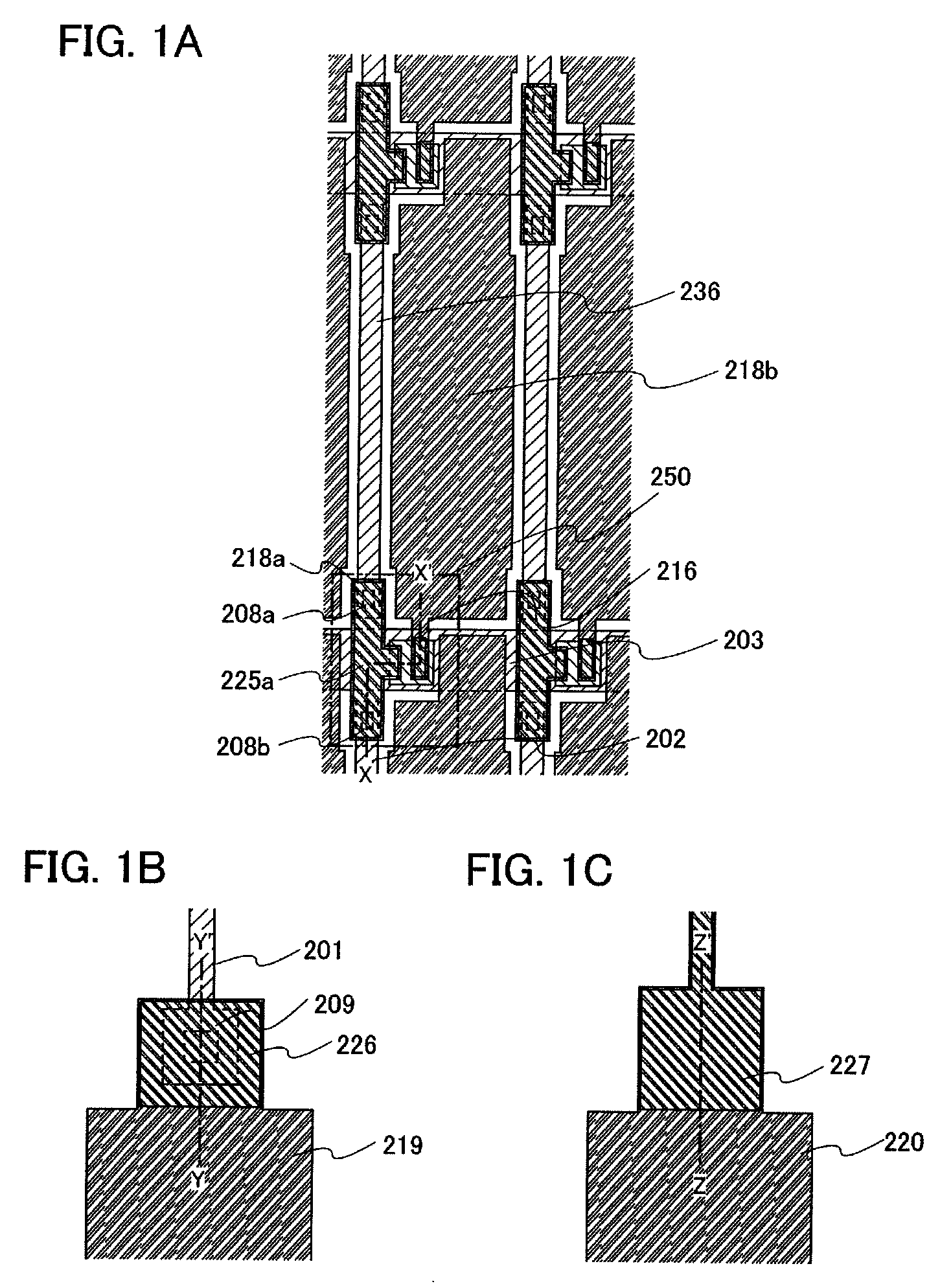
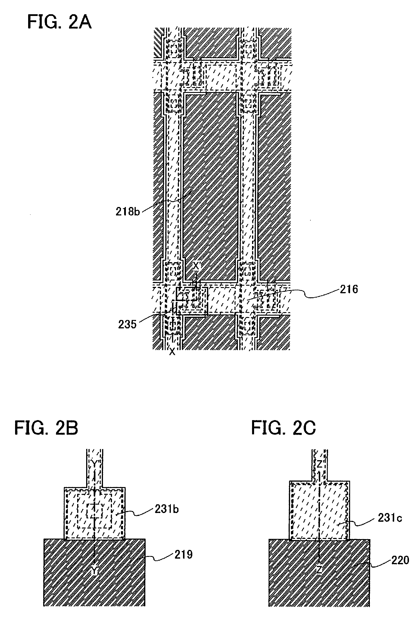
[0035]FIGS. 1A to 1C and FIGS. 2A to 2C show an example of a plane view which illustrates a display device includin...
embodiment mode 2
[0097]In this embodiment mode, an example of a thin film transistor whose shape is different from that of Embodiment Mode 1 will be described. Except the shape, the thin film transistor can be formed in a similar manner to Embodiment Mode 1; thus, repetitive description of the same components or components having similar functions as in Embodiment Mode 1 and a manufacturing process for forming those components will be omitted.
[0098]A thin film transistor 240 of this embodiment mode, which is an inversed staggered thin film transistor with a channel-etched structure, is shown in FIG. 8.
[0099]In FIG. 8, over a substrate 248a, thin film transistor 240 is provided, which includes a gate electrode layer 241, a gate insulating layer 242, a semiconductor layer 243, which is a microcrystalline semiconductor film, a buffer layer 244, source or drain regions 245a and 245b, light-transmitting conductive layers 246a and 246b, and conductive layers 247a and 247b. An insulating film 249 is provid...
embodiment mode 3
[0130]In this embodiment mode, an example of a manufacturing process of Embodiment Mode 2, in which a microcrystalline semiconductor film is irradiated with a laser beam, will be described.
[0131]A gate electrode layer is formed over a light-transmitting substrate, and a gate insulating layer is formed to cover the gate electrode layer. Then, a microcrystalline silicon (SAS) film is deposited over the gate insulating layer as a microcrystalline semiconductor film. The thickness of the microcrystalline semiconductor film may be greater than or equal to 1 nm and less than 15 nm, preferably greater than or equal to 2 nm and less than or equal to 10 nm. In particular, since the microcrystalline semiconductor film with a thickness of 5 nm (4 nm to 8 nm) has high absorptance with respect to a laser beam, productivity is improved.
[0132]In the case where the microcrystalline semiconductor film is formed over the gate insulating layer by a plasma CVD method or the like, a region which include...
PUM
 Abstract
Description
Claims
Application Information