Interlayer Insulating Film, Interconnection Structure, and Methods of Manufacturing the Same

a technology of interconnection structure and insulating film, which is applied in the direction of solid-state devices, basic electric elements, chemistry apparatus and processes, etc., can solve the problems of poor adhesion, low permittivity, and inability to detect the interconnection resistance, so as to reduce the outgasing of sif-based gases, prevent the stripping of the fluorocarbon film, and reduce the effect of permittivity

Inactive Publication Date: 2009-04-30
TOHOKU UNIV +1
View PDF18 Cites 18 Cited by
  • Summary
  • Abstract
  • Description
  • Claims
  • Application Information

AI Technical Summary

Benefits of technology

[0039]According to this invention, it is possible to provide an interlayer insulating film of a semiconductor device, which has a low permittivity, is free from generation of gases such as CFx and SiF4, and is stable, and a method of manufacturing it.
[0040]Further, according to this invention, it is possible to provide an interconnection structure comprising such an interlayer insulating film and a method of manufacturing it.
[0041]Further, according to this invention, by first forming a fluorocarbon film by plasma CVD using a Xe or Kr gas, it is possible to reduce outgassing of SiF-based gases and further to prevent stripping of the fluorocarbon film. Then, by forming a main portion of the fluorocarbon film by CVD in an Ar gas plasma, it is possible to reduce the effective permittivity of the fluorocarbon film.
[0042]Further, according to this invention, by nitriding the surface of the fluorocarbon film, there is an effect of largely reducing outgassing and there is also an effect of preventing stripping of an insulating film formed on the fluorocarbon film.
[0043]Further, according to this invention, by providing a barrier layer of nickel difluoride on the inner surface of a via hole or a contact hole, it is possible to prevent Cu in the hole from diffusing into the barrier layer.

Problems solved by technology

In such a multilayer interconnection structure, a problem of signal delay due to the parasitic capacitance between interconnections and the interconnection resistance has become unignorable and it has been required to use an interlayer insulating film having a low permittivity (Low-k).
However, the CFx film is very weak against water and poor in adhesion.
Therefore, the CF film is formed on an underlayer such as an SiCN layer, an Si3N4 layer, or an SiO2 layer, but there has been a problem in the bottom and top surfaces of the CF film (i.e. the beginning and end of the film formation).
As described in Patent Document 2, this CFx gas is originally used for etching and thus there has been a problem that if the plasma treatment temperature is high, an underlayer is etched to produce a silicon fluoride (SiF4) gas.
Further, there has been a problem that water and gases such as CFx and SiF4 are released from the surface of the formed CF film to form a contamination source.

Method used


Image

  • Interlayer Insulating Film, Interconnection Structure, and Methods of Manufacturing the Same
  • Interlayer Insulating Film, Interconnection Structure, and Methods of Manufacturing the Same
  • Interlayer Insulating Film, Interconnection Structure, and Methods of Manufacturing the Same

Examples


Embodiment Construction

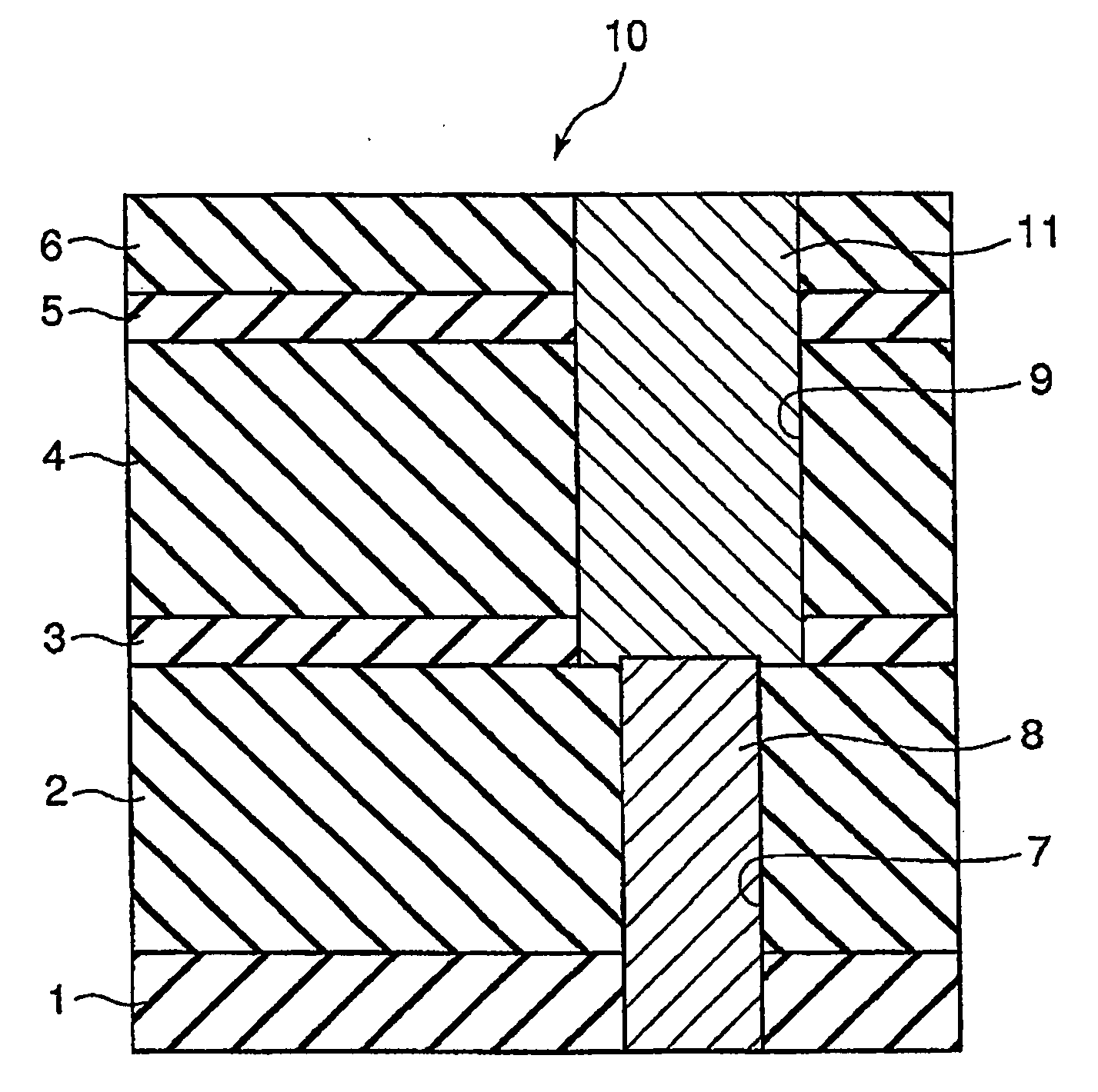
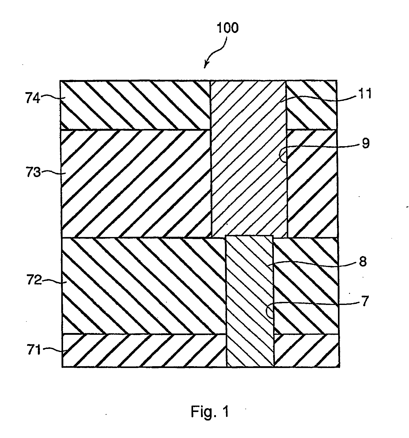
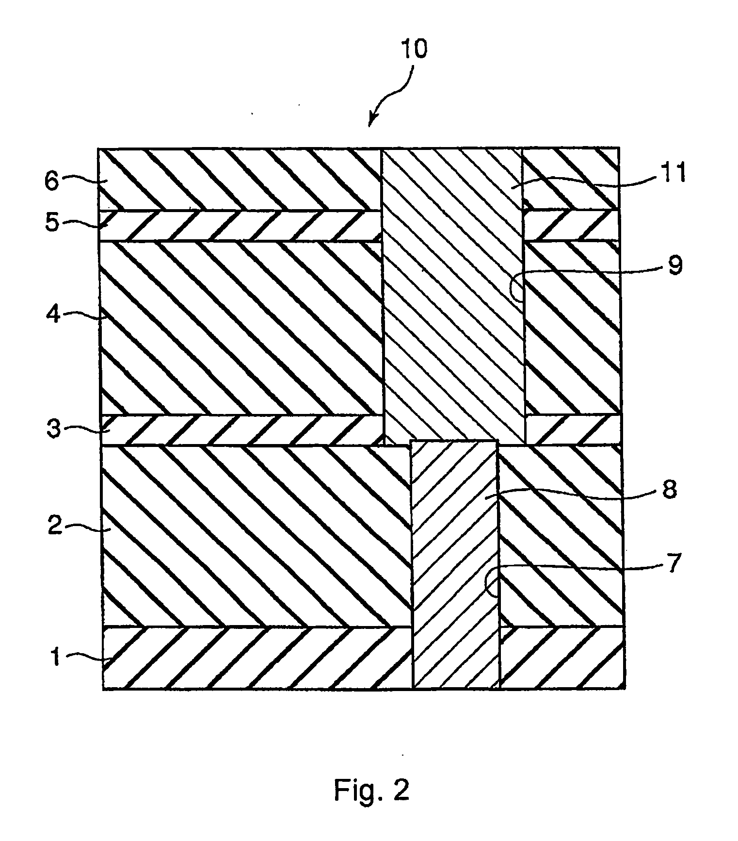
[0142]In order to facilitate understanding of this invention, a conventional interlayer insulating film structure of a semiconductor device according to prior art will be described with reference to FIG. 1 before describing an embodiment of this invention.

[0143]Referring to FIG. 1, in the semiconductor device according to prior art, an interlayer insulating film structure (only one connecting portion between interconnection layers is shown) 100 provided on a semiconductor substrate (not shown) formed with a number of semiconductor elements comprises a barrier cap layer 71 of silicon carbide (SiC) or the like, a carbon-containing silicon oxide (SiOC) film 72 formed on the barrier cap layer 71, a via hole 8 provided in the SiOC film 72, a trench 9 provided in a PAR (low-permittivity silicon (Si) layer 73), and a hard mask 74 of silicon oxide (SiO2) covering them. A metal such as Cu is buried in the via hole 8 to form an electrode or interconnection 8 and, at its upper end, Cu or the l...


PUM

PropertyMeasurementUnit
thicknessaaaaaaaaaa
thicknessaaaaaaaaaa
thicknessaaaaaaaaaa

Abstract

This invention provides an interlayer insulating film for a semiconductor device, which has low permittivity, is free from the evolution of gas such as CFx and SiF4 and is stable, and a wiring structure comprising the same. In an interlayer insulating film comprising an insulating film provided on a substrate layer, the interlayer insulating film has an effective permittivity of not more than 3. The wiring structure comprises an interlayer insulating film, a contact hole provided in the interlayer insulating film, and a metal filled into the contact hole. The insulating film comprises a first fluorocarbon film provided on the substrate layer and a second fluorocarbon film provided on the first fluorocarbon film.

Description

TECHNICAL FIELD[0001]This invention relates to a multilayer interconnection structure, particularly an interlayer insulating film structure, of a board, such as a semiconductor-element or semiconductor-chip mounting board or a wiring board and further relates to a semiconductor device having the multilayer interconnection structure, a wiring board having the multilayer interconnection structure, and an electronic device including them. Moreover, this invention relates to a method of manufacturing the multilayer interconnection structure and methods of manufacturing the semiconductor device having the multilayer interconnection structure, the wiring board having the multilayer interconnection structure, and the electronic device including them.BACKGROUND ART[0002]Conventionally, an interlayer insulating film is formed for insulation between interconnection layers in a multilayer interconnection structure on a semiconductor substrate or the like.[0003]In such a multilayer interconnect...

Claims


Application Information

Patent Timeline
Patent Type & Authority Applications(United States)
IPC IPC(8): H01L23/522H01L23/00H01L21/31H01L23/488H01L21/768
CPCH01L21/0212H01L21/02274H01L21/02329H01L21/0234H01L21/02362H01L21/3127H01L21/76835H01L2924/0002H01L23/49894H01L23/5329H01L23/53295H01L2924/00
Inventor OHMI, TADAHIRO
Owner TOHOKU UNIV
Why Eureka
Try Eureka