Plasma electron flood for ion beam implanter

a technology of plasma electron flood and implanter, which is applied in the field of ion implantation systems, can solve the problems of gate oxide damage, microwave and rf discharge, and increase the cost of individual workpieces

Active Publication Date: 2009-05-07
AXCELIS TECHNOLOGIES
View PDF17 Cites 23 Cited by
  • Summary
  • Abstract
  • Description
  • Claims
  • Application Information

AI Technical Summary

Benefits of technology

[0033]The following presents a simplified summary in order to provide a basic understanding of one or more aspects of the invention. This summary is not an extensive overview of the invention, and is neither intended to identify key or critical elements of the invention, nor to delineate the scope thereof. Rather, the primary purpose of the summary is to present some concepts of the invention in a simplified form as a prelude to the more detailed description that is p

Problems solved by technology

This effect, commonly referred to as charging, can be detrimental to the semiconductor circuit if the voltages of the insulated feature (e.g. the gate electrode) exceed the breakdown voltage of the insulator (e.g. the gate oxide) such that resultant damage to the gate oxide occurs.
It can be appreciated that the charging rate and voltage increase with beam current, and that ion implantation with ever increasing beam currents represents an increasing processing challenge.
Coupled with higher device densities, the larger workpie

Method used


Image

  • Plasma electron flood for ion beam implanter
  • Plasma electron flood for ion beam implanter
  • Plasma electron flood for ion beam implanter

Examples


Embodiment Construction

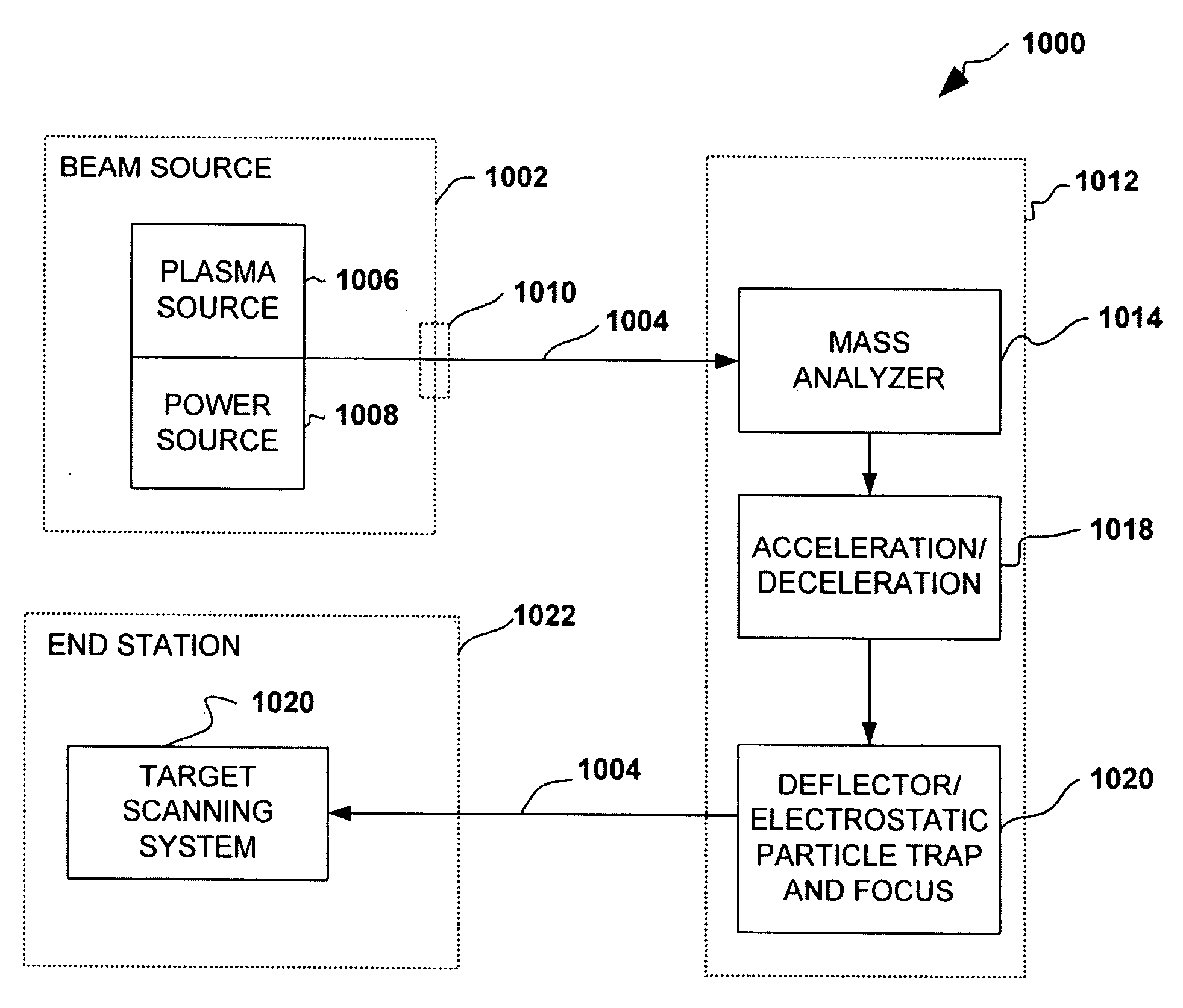
[0052]The present invention will now be described with reference to the drawings wherein like reference numerals are used to refer to like elements throughout. The invention provides methods and systems for provision of a plasma electron flooded ion beam for ion implantation of workpieces such as semiconductor workpieces. One implementation of the invention is illustrated and described hereinafter with respect to the drawing figures. The illustrations and following descriptions are exemplary in nature, and not limiting. Thus, it will be appreciated that variants of the illustrated systems and methods and other such implementations apart from those illustrated herein are deemed as falling within the scope of the present invention and the appended claims.

[0053]Referring initially to FIG. 8 the figure illustrates an exploded partial view of the invention which provides a plasma electron flood system (PEF) 800 comprising a housing 802 configured to contain a gas introduced by e.g., a va...


PUM


Abstract

A plasma electron flood system, comprising a housing configured to contain a gas, and comprising an elongated extraction slit, and a cathode and a plurality of anodes residing therein and wherein the elongated extraction slit is in direct communication with an ion implanter, wherein the cathode emits electrons that are drawn to the plurality of anodes through a potential difference therebetween, wherein the electrons are released through the elongated extraction slit as an electron band for use in neutralizing a ribbon ion beam traveling within the ion implanter.

Description

FIELD OF THE INVENTION[0001]The present invention relates generally to ion implantation systems, and more particularly to uniform charge neutralization of an ion beam utilized in ion implantation systems.BACKGROUND OF THE INVENTION[0002]Ion implantation systems are used to dope semiconductors with impurities in integrated circuit manufacturing. In such systems, an ion source ionizes a desired dopant element, which is extracted from the source in the form of an ion beam of desired energy. The ion beam is then directed at the surface of a semiconductor workpiece in order to implant the workpiece with the dopant element. The ions of the beam penetrate the surface of the workpiece to form a region of desired conductivity, such as in the fabrication of transistor devices in the workpiece or wafer. The implantation process is typically performed in a high vacuum process chamber which prevents dispersion of the ion beam by collisions with residual gas molecules and which minimizes the risk...

Claims


Application Information

Patent Timeline
IPC IPC(8): H01J37/317B05C5/02H01J17/16
CPCH01J37/026H01J2237/06366H01J2237/0041H01J37/3171
Inventor VANDERBERG, BO H.DIVERGILIO, WILLIAM F.
Owner AXCELIS TECHNOLOGIES
Why Eureka
Try Eureka