Semiconductor range-finding element and solid-state imaging device

a range-finding element and solid-state imaging technology, applied in the direction of radiation controlled devices, distance measurement, instruments, etc., can solve the problems of low random noise level, inability to reset noise, and difficulty in solving the reduction of dark current, so as to improve the low noise performance and reduce the dark current. , the effect of reducing the manufacturing cos

Active Publication Date: 2009-05-07
SHARP KK
View PDF8 Cites 63 Cited by
  • Summary
  • Abstract
  • Description
  • Claims
  • Application Information

AI Technical Summary

Benefits of technology

[0007]It is therefore an object of the present invention to provide a semiconductor range-finding element that can be manufactured at a low manufacturing cost and is superior in low noise performance which is achieved by a smaller dark current and a removal of reset noise, and further to provide a solid-state imaging device that uses the semiconductor range-finding element as one of a plurality of pixels and has a high distance resolution and a space resolution.

Problems solved by technology

However, in an approach of the method of using, as an active layer, the semiconductor layer under the field oxide film proposed in JP 2005-235893A, a dark current was large, and the reduction of the dark current was a problem to be solved.
Also, in an approach of accumulating the charges in the floating diffusion layer such as the structure proposed in JP 2004-294420A, the approach had problems such that reset noise could not be removed, a random noise level was high, and the performance deterioration was severe in the region in which light quantity was small.
However, the use of various insulating films other than the silicon oxide film (SiO2 film) is not inhibited.
However, the lack of the thermal stability on the interface with the poly-crystalline silicon and the hysteresis characteristic of the ferroelectric material are required to be considered.

Method used


Image

  • Semiconductor range-finding element and solid-state imaging device
  • Semiconductor range-finding element and solid-state imaging device
  • Semiconductor range-finding element and solid-state imaging device

Examples


first embodiment

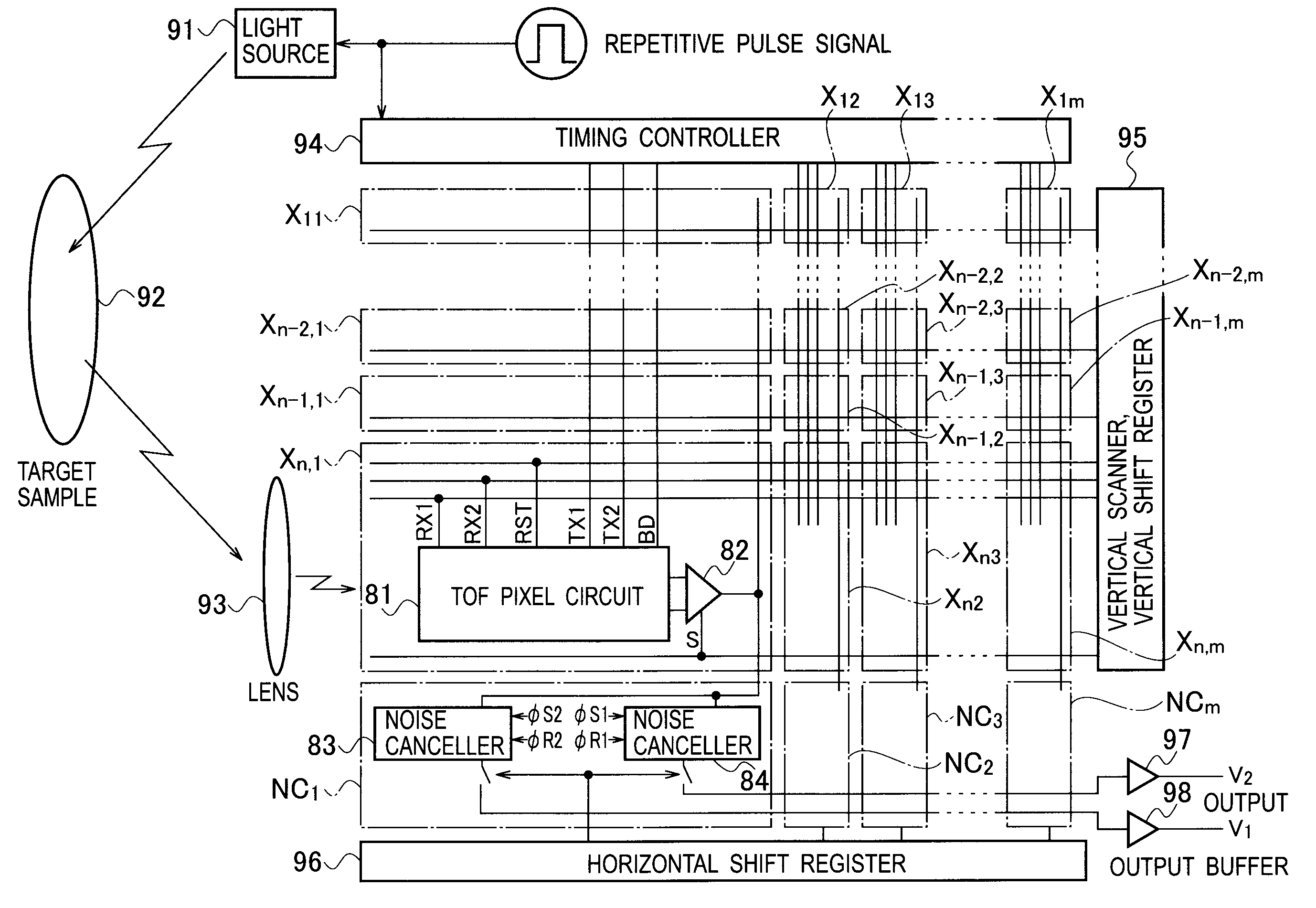
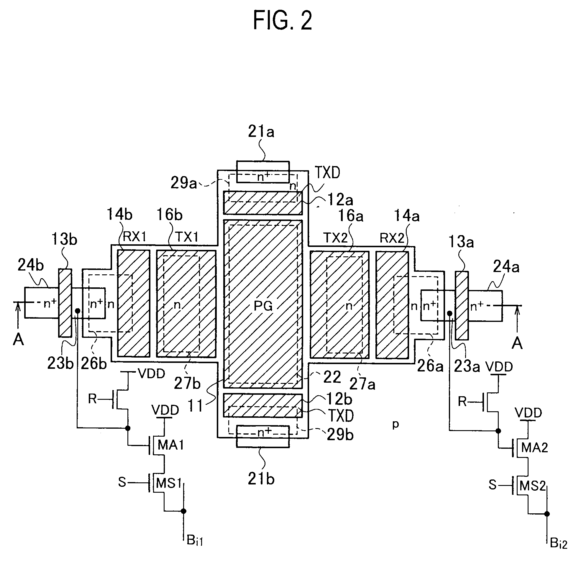
[0038]In a solid-state imaging device (two-dimensional image sensor) according to a first embodiment of the present invention, as shown in FIG. 1, a pixel array area (X1l to X1m, X2l to X2m, - - -Xn1 to Xnm) and peripheral circuit areas (94, 95, 96, and NC1 to NCm) are merged on a same semiconductor chip. A large number of pixels Xij (i=1 to m, j=1 to n, and the m, n are integers, respectively) are two-dimensionally arrayed in the pixel array area, and a rectangular imaging area is established. Then, a timing controller 94 is provided on the upper side of the pixel array area, and a horizontal shift register 96 is provided on the lower side, respectively along pixel rows X11 to X1m, X21 to X2m, - - - , Xn1 to Xnm directions. On the right side of the pixel array area, a vertical shift register and a vertical scanning circuit 95 are provided along pixel columns X11 to Xn1, X12 to Xn2, - - - , X1j to Xnj, - - - X1m to Xnm directions. As an inner structure of the pixel Xnj is representa...

second embodiment

[0082]The entire configuration of the solid-state imaging device (two-dimensional image sensor) according to a second embodiment of the present invention is equal to the block diagram shown in FIG. 1. Thus, the duplex explanations are omitted. Also, the planar configuration of a semiconductor range-finding element serving as a TOF pixel circuit 81 assigned in each of the pixels X11 to X1m, X21 to X2m, - - - , Xn1 to Xnm in the solid-state imaging device pertaining to the second embodiment is basically similar to the planar configuration shown in FIG. 2, which has been shown as one example of the planar configuration of the semiconductor range-finding element pertaining to the first embodiment, with regard to the pattern of the surface wirings delineated on the insulating film 31. Hence, the duplex explanations are omitted.

[0083]FIG. 8 is the sectional structure of the semiconductor range-finding element shown in FIG. 2. Although, the configuration such that the semiconductor range-f...

third embodiment

[0118]The entire structure of the solid-state imaging device (two-dimensional image sensor) pertaining to the third embodiment of the present invention is basically equal to the block diagram shown in FIG. 1. Thus, the duplex explanations are omitted.

[0119]The sectional structure of the semiconductor range-finding element serving as the TOF pixel circuit 81 assigned in each of the pixels X11 to X1m; X21 to X2m; - - - ; Xn1 to Xnm in the solid-state imaging device pertaining to the third embodiment is basically similar to the sectional structure of the semiconductor range-finding element pertaining to the first embodiment. However, the planar layout differs from the planar configuration of the semiconductor range-finding element pertaining to the first embodiment. That is, in the first embodiment, as shown in FIG. 2, the pixel structure is illustrated in which the first transfer gate electrode 16b and the second transfer gate electrode 16a are provided on both of the sides of the lig...


PUM


Abstract

A semiconductor range-finding element and a solid-state imaging device, which can provide a smaller dark current and a removal of reset noise. With n-type buried charge-generation region, buried charge-transfer regions, buried charge read-out regions buried in a surface of p-type semiconductor layer, an insulating film covering these regions, transfer gate electrodes arranged on the insulating film for transferring the signal charges to the buried charge-transfer regions, read-out gate electrodes arranged on the insulating film for transferring the signal charges to the buried charge read-out regions, after receiving a light pulse by the buried charge-generation region, in the semiconductor layer just under the buried charge-generation region, an optical signal is converted into signal charges, and a distance from a target sample is determined by a distribution ratio of the signal charges accumulated in the buried charge-transfer regions.

Description

FIELD OF THE INVENTION[0001]The present invention relates to a semiconductor range-finding element and a solid-state imaging device in which a plurality of semiconductor range-finding elements are arrayed.DESCRIPTION OF THE RELATED ART[0002]As reported by R. Miyagawa et al., “CCD-Based Range-Finding Sensor”, IEEE Transaction on Electron Devices, October 1997, Vol. 44, No. 10, pp. 1648-1652, with a pioneering report of one-dimensional CCD range-finding sensor, which has been firstly reported in 1997, the development of time-of-flight (TOF) type range-finding sensors using time-of-flight of light and obtaining range images are advancing in many fields.[0003]However, the resolution of the currently available TOF type range-finding sensor remains within about 20,000 pixels. Also, in the case of a method of using the CCD, as the number of the pixels is increased, it becomes difficult to drive the pixels. In the method of using the mixture process of CMOS and CCD, its manufacturing cost b...

Claims


Application Information

Patent Timeline
Patent Type & Authority Applications(United States)
IPC IPC(8): H01L31/10H01L27/148G01S17/894H04N5/357
CPCG01C3/02G01C3/08G01S7/4816G01S17/89H04N5/3575H01L27/14609H01L27/14643H01L27/14689H01L31/02024H01L27/14603G01S17/894H04N25/616
Inventor KAWAHITO, SHOJIWATANABE, TAKASHI
Owner SHARP KK
Why Eureka
Try Eureka