Semiconductor light-emitting device with a surface emitting type

a surface-emitting, semiconductor-type technology, applied in semiconductor lasers, laser details, electrical devices, etc., can solve the problems of reducing the emission efficiency, reducing the parasitic capacitance of the device, and limited high-frequency performance of the device, so as to increase the flexibility of the device design

Inactive Publication Date: 2009-05-07
SUMITOMO ELECTRIC IND LTD
View PDF5 Cites 6 Cited by
  • Summary
  • Abstract
  • Description
  • Claims
  • Application Information

AI Technical Summary

Benefits of technology

[0012]Because the un-doped GaInP or the AlGaInP of the current blocking layer is grown at a low temperature between 500 to 600° C., or between 500 to 650° C., these layers may contain deep levels to trap both electrons and holes, an additional layer to trap holes becomes unnecessary which increases the flexibility of the device design, specifically, the design of the layer configuration of the device.

Problems solved by technology

However, irons do not show the trap function for holes; accordingly, it is inevitable to put an additional layer between the Fe-doped layer and the p-type layer, ordinarily the p-type cladding layer, to trap holes when the Fe-doped layer is applied to the current blocking layer in the laser diode, which increases the parasitic capacitance of the device, especially, between the cladding layer and the current blocking layer, and the high-frequency performance of the device is limited.
This inter-diffusion between Fe and Zn reduces the resistivity in the Fe-doped layer, while, the resistivity of the p-type layer is raised, which increases not only the leak current flowing in the blocking layer to lower the emission efficiency but the parasitic capacitance thereat to limit the high frequency performance of the device.

Method used


Image

  • Semiconductor light-emitting device with a surface emitting type
  • Semiconductor light-emitting device with a surface emitting type
  • Semiconductor light-emitting device with a surface emitting type

Examples


first embodiment

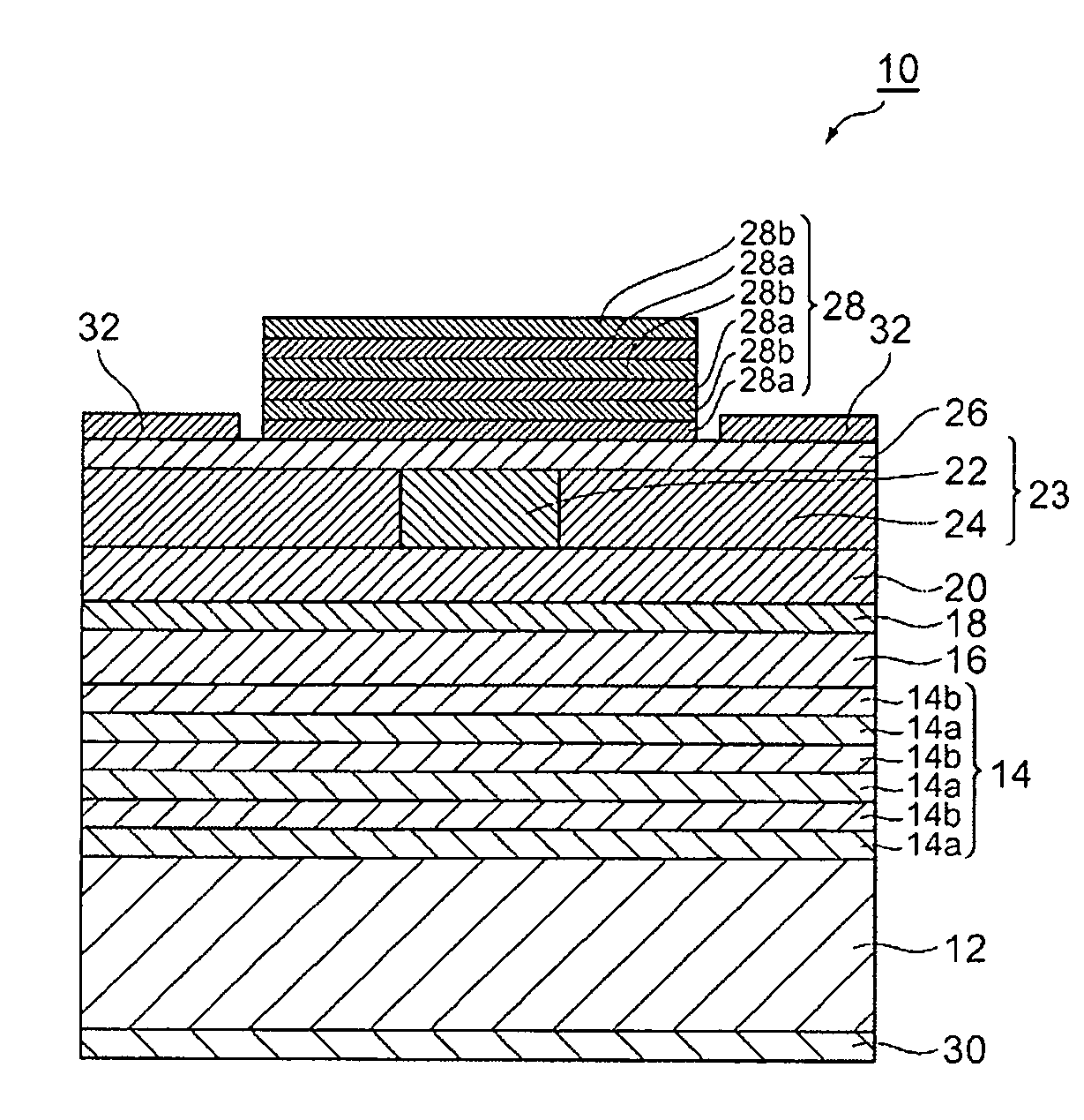
[0028]FIG. 1 is a cross section of an optical device with a type of the surface emitting according to the first embodiment of the invention. The surface emitting device 10 shown in FIG. 1 may be, for instance, a vertical cavity surface emitting laser diode (VCSEL), where the device 10 provides a first distributed Bragg Reflector (DBR) structure 14 with the first conductivity type on an n-type GaAs substrate 12, an active layer 18 provided on the first DBR structure 14, a current injecting layer 22 with a second conduction type, for instance the p-type, and provided on the first DBR structure to inject carriers into the active layer 18, a second DBR structure 28 provided on the current injecting layer 22, and a current blocking layer 28 provided between the first and second DBR structures, 14 and 28, respectively. This current blocking layer 24 is formed in the sides of the current injecting layer 22, and made of un-doped GaInP or un-doped AlGaInP. The current injecting layer 22 and ...

second embodiment

[0075]FIG. 7 is a cross section of an optical device with the surface emitting type according to a second embodiment of the invention. The optical device 10a shown in FIG. 7 provides, in addition to the layer configuration the optical device 10 in the first embodiment, an intermediate layer 40 with the second conduction type between the current confinement structure 23 and the upper spacer layer 20. This intermediate layer 40 may be made of GaAs, AlGaAs, or GaInAsP.

[0076]The process to form the optical device 10a will be described.

[0077]First, the process grows a series of semiconductor layers of the first DBR structure 14, the space layer 16, the active layer 18, the upper spacer layer 20, the intermediate layer 40 and the current injection layer 22a on the GaAs substrate 12 in this order. The OMVPE technique may also carry out the growth.

[0078]Next, the dielectric film 34 is formed on the current injection layer 22a.

[0079]Similar to the process shown in FIG. 4C, the process etche...

third embodiment

[0083]FIG. 8 is a cross section of an optical device with the surface emitting type according to the third embodiment of the invention. The optical device 10b shown in FIG. 8 provides, in addition to those appeared in the optical device 10 of the first embodiment, an intermediated layer 42 with the second conduction type only between the current injection layer 22 and the upper spacer layer 20. This intermediate layer 42 may be made of the same material with the intermediate layer 40 in the second embodiment. The optical device shown in FIG. 8 does not provide the intermediate layer 42 between the current blocking layer 24 and the upper spacer layer 20.

[0084]Because the intermediate layer 42 exists only between the current injection layer 22 and the spacer layer 20, it is possible by adjusting a characteristic of this intermediate layer 42 to improve the performance of the optical device 10b. The intermediate layer 42 may be made of semiconductor material whose refractive index is g...


PUM


Abstract

A structure of an optical device with the surface emitting type and a method to form the optical device are disclosed, where the optical device is able to operate in high frequencies. The device provides a lower DBR structure, an active layer, a current injection layer, a current blocking layer, and an upper DBR structure on a GaAs substrate. The current blocking layer, horizontally putting the current injection layer therebetween, are an un-doped GaInP grown at a temperature between 500 to 600° C. and an un-doped AlGaInP grown at a temperature between 500 to 650° C. Because the un-doped current blocking layer shows the high resistivity for both electrons and holes, the parasitic capacitance in the current blocking layer becomes small.

Description

CROSS-REFERENCE TO RELATED APPLICATIONS[0001]The contents of the present application closely relates to applications, serial numbers of which are Ser. No. 11 / 889,613, filed Aug. 15, 2007, entitled by “Semiconductor laser diode with a mesa stripe buried by a current blocking layer made of un-doped semiconductor grown at a low temperature and a method for producing the same”, and Ser. No. 11 / 889,461, filed Aug. 13, 2007, entitled by “Semiconductor laser diode with a ridge structure buried by a current blocking layer made of un-doped semiconductor grown at a low temperature and a method for producing the same”, which are incorporated herein by reference in their entirely.BACKGROUND OF THE INVENTION[0002]1. Field of the Invention[0003]The present invention relates to a semiconductor optical device, in particular, the invention relates to a semiconductor laser diode with a vertical cavity surface emitting type.[0004]2. Related Prior Art[0005]A semiconductor laser diode with a type of ver...

Claims


Application Information

Patent Timeline
Patent Type & Authority Applications(United States)
IPC IPC(8): H01S5/183H01L21/02
CPCH01S5/18308H01S5/18358H01S2301/173H01S5/2209H01S5/32366H01S5/18369
Inventor HASHIMOTO, JUN-ICHI
Owner SUMITOMO ELECTRIC IND LTD
Why Eureka
Try Eureka