Stress-generating shallow trench isolation structure having dual composition

a technology of isolation structure and stress generation, which is applied in the direction of electrical equipment, semiconductor devices, semiconductor/solid-state device details, etc., can solve the problems of disadvantageous to the enhancement of performance of pmosfet, no mechanism is provided to reverse the stress direction, and the magnitude of stress tends to decay rapidly, so as to achieve different stress-generating properties, enhance charge carrier mobility, and enhance the effect of stress generation

Active Publication Date: 2009-05-21
MARVELL ASIA PTE LTD
View PDF99 Cites 25 Cited by
  • Summary
  • Abstract
  • Description
  • Claims
  • Application Information

AI Technical Summary

Benefits of technology

[0009]The present invention addresses the needs described above by providing a semiconductor structure including a shallow trench isolation structure having a dual composition in which a first shallow trench isolation structure portion and a second shallow trench isolation structure portion have different composition and have different stress-generating properties. Methods of manufacturing such a semiconductor structure are also provided.
[0010]In the present invention, an etch stop layer having etch selectivity to a first shallow trench isolation material is formed on a top surface of a semiconductor substrate. A shallow trench surrounding at least one first active area for forming a first conductivity type transistor, which may be a p-type transistor or an n-type transistor, and at least one second active area for forming an opposite conductivity type transistor is formed. The shallow trench is filled with a first shallow trench isolation material which has a first composition and first stress generating properties.
[0011]A photoresist is applied over the at least one first active area and the at least one second active area and patterned such that a portion of the first shallow trench isolation material is exposed from a middle portion of the at least one first active area and from edge portions of the at least one second active area. Exposed portions of the first shallow trench isolation material is removed by an anisotropic etch that is selective to the etch stop layer. Cavities, which are formed by removal of the first shallow trench isolation material, are filled with a second shallow trench isolation material which has a second composition and second stress-generating properties. The second shallow trench isolation material is then planarized.
[0012]A shallow trench isolation structure containing a first shallow trench isolation portion comprising the first shallow trench material and a second shallow trench isolation portion comprising the second shallow trench material is thus formed. A first biaxial stress on the at least one first active area and a second bidirectional stress on the at least one second active area are manipulated separately to enhance charge carrier mobility in middle portions of the at least one first and second active areas by selection of the first and second shallow trench materials as well as adjusting the type of the shallow trench isolation material that each portion of the at least one first active area and the at least one second active area laterally abut. The etch stop layer is removed, and a channel and a gate stack are thereafter formed on each of the at least one first and second active areas that are subjected to different types of biaxial stress. The enhanced charge carrier mobility of the middle portion of the at least one first and second active areas is advantageously employed to provide enhanced performance of both types of field effect transistors.
[0013]According to an aspect of the present invention, a semiconductor structure is provided, which comprises:
[0014]an active area comprising a semiconductor material and located in a semiconductor substrate;

Problems solved by technology

Prior art stress-generating structures such as stress-generating liners formed above a semiconductor substrate and on a gate line is inefficient in transmission of a stress to a channel region of a transistor since the stress is transmitted through gate spacers, and the magnitude of the stress tends to decay rapidly with depth into the semiconductor substrate.
Further, in the case of a PMOSFET, no mechanism is provided for reversing the direction of stress between the longitudinal stress and the transverse stress.
In other words, if the longitudinal stress is compressive and beneficial to enhance of performance of the PMOSFET, the transverse stress is also compressive, which is disadvantageous to enhancement of performance of the PMOSFET.

Method used


Image

  • Stress-generating shallow trench isolation structure having dual composition
  • Stress-generating shallow trench isolation structure having dual composition
  • Stress-generating shallow trench isolation structure having dual composition

Examples


first embodiment

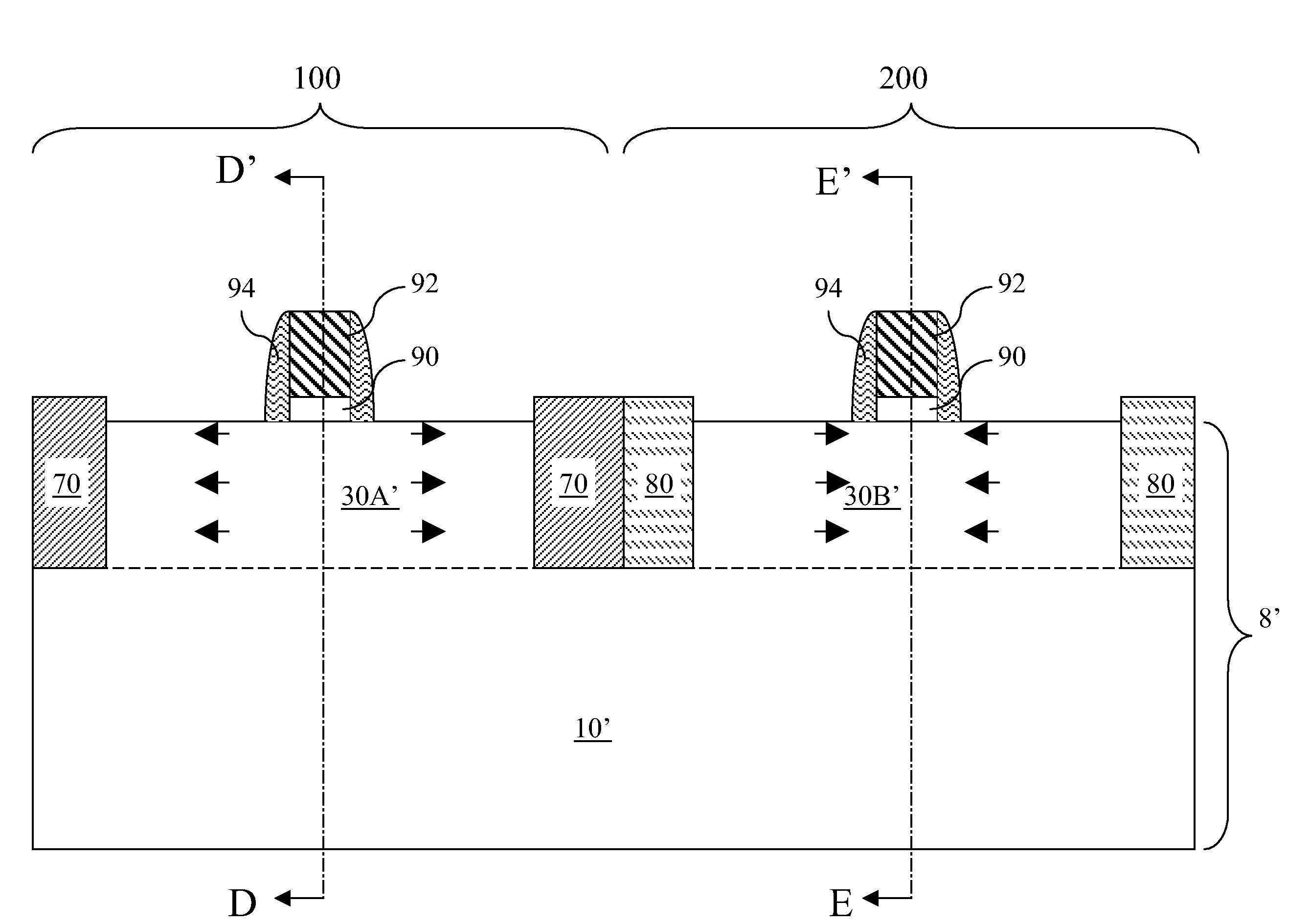
[0117]As in the first embodiment, a first channel C1 is formed in each of the middle portion of the at least one first active area 30A that vertically abuts a gate dielectric 90 in the first device region 100. The first shallow trench isolation portion 70 comprising the first shallow trench isolation material applies a first longitudinal stress along a lengthwise direction in the first channel C1 and a first transverse stress along a widthwise direction of the first channel C1.

[0118]A second channel C2 is formed in each of the middle portion of the at least one second active area 30B that vertically abuts a gate dielectric 90 in the second device region 100. The shallow trench isolation structure (70, 80) comprising the first shallow trench isolation portion 70 and the second shallow trench isolation portion 80 applies a second longitudinal stress along a lengthwise direction in the second channel C2 and a first transverse stress along a widthwise direction of the second channel C2....

third embodiment

[0123]Referring to FIG. 9A, a result of a simulation for longitudinal stress and transverse stress distribution at the center of a channel of an n-type field effect transistor according to the present invention is shown. The simulation assumes a nested array of first active areas comprising silicon and having a width of 100 nm and a depth of 400 nm, which is the same as the depth of the first shallow trench isolation portion 70 and the second shallow trench isolation portion 80. Each of the first active areas constitutes an instance of the n-type field effect transistor. The first shallow trench isolation portion 70 comprises a tensile-stress-generating silicon nitride, which applies a tensile stress of about 1.5 GPa to surrounding regions that abut the first shallow trench isolation portion 70. The second shallow trench isolation portion 80 comprises a silicate glass and has an inherent stress level less than 100 MPa, and typically less than about 30 MPa.

[0124]The third exemplary s...

fourth embodiment

[0127]Referring to FIG. 9C, a result of a simulation for an n-type field effect transistor according to the present invention is shown. The simulation assumes a nested array of first active areas comprising silicon and having a width of 100 nm and a depth of 400 nm, which is the same as the depth of the first shallow trench isolation portion 70 and the second shallow trench isolation portion 80. In this case, the first shallow trench isolation portion 70 completely surrounds each of the first active areas, which constitutes an instance of the n-type field effect transistor. The first shallow trench isolation portion 70 comprises a tensile-stress-generating silicon nitride, which applies a tensile stress of about 1.5 GPa to surrounding regions that abut the first shallow trench isolation portion 70.

[0128]The fourth exemplary semiconductor structure generates a longitudinal tensile stress from about 800 MPa to about 1,400 MPa and a transverse tensile stress from about 0 MPa to about 1...


PUM


Abstract

A shallow trench isolation structure containing a first shallow trench isolation portion comprising the first shallow trench material and a second shallow trench isolation portion comprising the second shallow trench material is provided. A first biaxial stress on at least one first active area and a second bidirectional stress on at least one second active area are manipulated separately to enhance charge carrier mobility in middle portions of the at least one first and second active areas by selection of the first and second shallow trench materials as well as adjusting the type of the shallow trench isolation material that each portion of the at least one first active area and the at least one second active area laterally abut.

Description

FIELD OF THE INVENTION[0001]The present invention relates to a stress-generating shallow trench isolation structure having a dual composition and methods of manufacturing the same.BACKGROUND OF THE INVENTION[0002]Manipulating stress is an effective way of improving charge carrier mobility in a metal oxide semiconductor field effect transistor (MOSFET) and increasing the transconductance (or reduced serial resistance) of the MOSFET that requires relatively small modifications to semiconductor processing while providing significant enhancement to MOSFET performance.[0003]When stress is applied to the channel of a semiconductor transistor, the mobility of carriers, and as a consequence, the transconductance and the on-current of the transistor are altered from their original values for an unstressed semiconductor. This is because the applied stress and the resulting strain on the semiconductor structure within the channel affects the band gap structure (i.e., breaks the degeneracy of t...

Claims


Application Information

Patent Timeline
Patent Type & Authority Applications(United States)
IPC IPC(8): H01L21/762H01L23/58H01L27/088
CPCH01L21/3081H01L21/31053H01L21/76224H01L21/823807H01L21/823878H01L2924/0002H01L27/092H01L29/7846H01L2924/00
Inventor ZHU, HUILONGWANG, JING
Owner MARVELL ASIA PTE LTD
Why Eureka
Try Eureka