Wiring board, method for manufacturing same and semiconductor device

a wiring board and resin technology, applied in the direction of resistive material coating, solid-state devices, metallic material coating process, etc., can solve the problems of increasing the demand for thinning wiring boards, difficulty in applying conventional methods, and wiring boards are prone to warping, etc., to suppress the warping of the entire wiring board, and reduce the cost of manufacturing

Inactive Publication Date: 2009-05-28
PANASONIC CORP
View PDF0 Cites 14 Cited by
  • Summary
  • Abstract
  • Description
  • Claims
  • Application Information

AI Technical Summary

Benefits of technology

[0017]Furthermore, the present invention includes a step of forming the wiring board which includes the electrically insulating base and wiring pattern, a step of forming the wiring protection layer on the surface and rear face of the wiring board, and a step of correcting warping at a temperature not less than the glass transition temperature of the electrically insulating base and the wiring protection layer. Thermal treatment at the temperature not less than the glass transition temperature of the electrically insulating base and wiring protection layer reduces an internal stress of the electrically insulating base and wiring protection layer. This results in eliminating a residual stress applied during the production steps, enabling correction of warping of the wiring board.
[0018]The present invention suppresses warping of the entire wiring board even when the wiring board is thin and is prone to warping. Consequently, the present invention offers the wiring board which achieves good electronic component mountability, and it manufacturing method.

Problems solved by technology

As a result, demands for thinning wiring boards are increasing.
Since the rigidity of these thin boards is lower, the wiring boards are prone to warping.
However, in the manufacturing process of wiring boards for board sizes of about 300 mm to 500 mm, curvature cannot be accurately controlled, resulting in difficulty in applying the conventional methods.
Accordingly, the stress in the thickness direction is not balanced locally, and this causes slight warping.
When product portions 1, which contain this slight warping respectively, are provided on the wiring board sheet, each slight warping accumulates, resulting in generating a large warping on a large sheet.
As a result, warping generated on the wiring board sheet has been causing failure in transport, low positional accuracy in mounting electronic components, and low mounting reliability in the electronic component mounting process.

Method used


Image

  • Wiring board, method for manufacturing same and semiconductor device
  • Wiring board, method for manufacturing same and semiconductor device
  • Wiring board, method for manufacturing same and semiconductor device

Examples


first exemplary embodiment

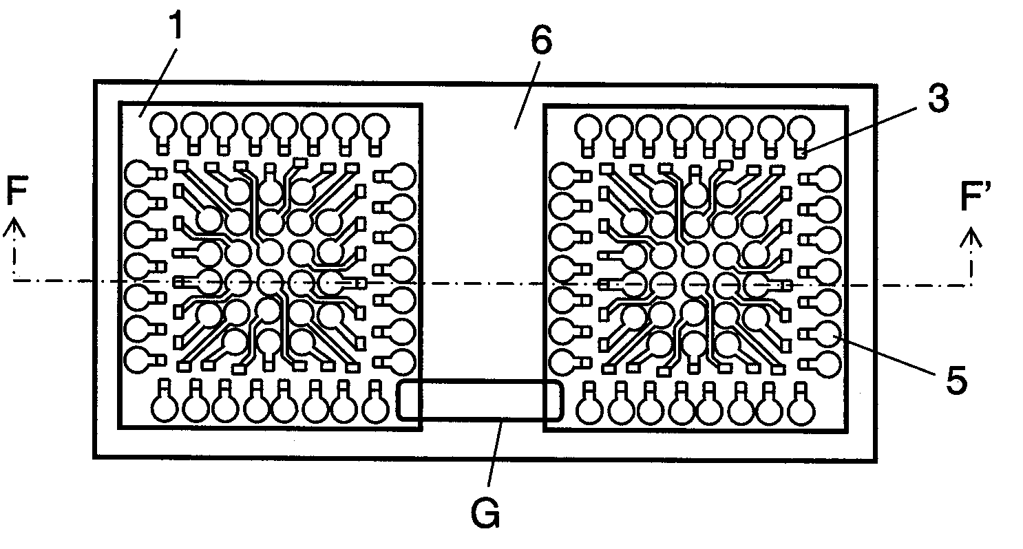
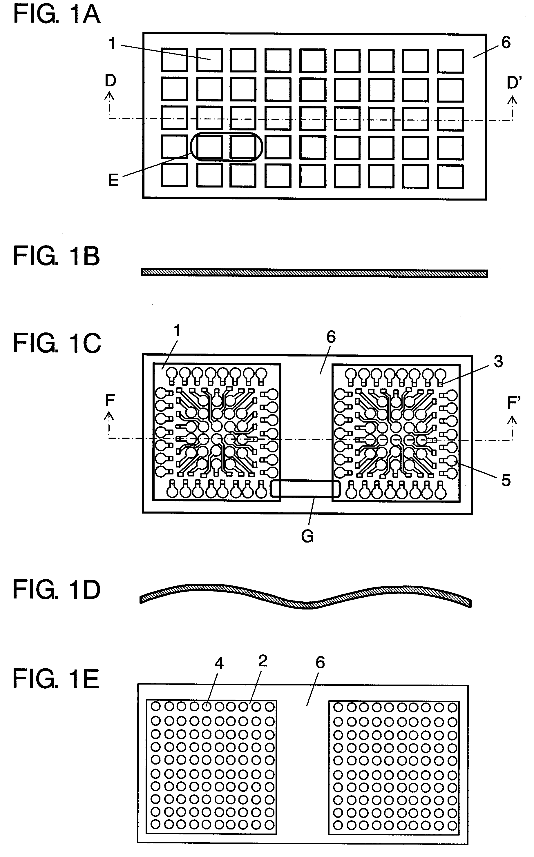
[0074]FIG. 1A illustrates the surface of a wiring board sheet. Product portion 1 is provided on a surface (first face) of the wiring board. A rear face of the wiring board is called the second face. Warp-correcting portion 6 is formed on an area other than product portion 1 of the wiring board sheet. FIG. 1A illustrates an example of providing multiple product portions on the wiring board sheet, but the concept of the present invention is also applicable to the case when single product portion 1 is provided on the wiring board sheet. Warp-correcting portion 6 is warped in a direction different from a warping direction of product portion 1. This suppresses significant warping of the wiring board caused by accumulation of warping of each product portion 1 when product portions 1 are continuously provided.

[0075]The warping direction is defined next. First, the center of gravity of individual product portion 1 is set as the origin, and the vertical axis and horizontal axis within the ar...

second exemplary embodiment

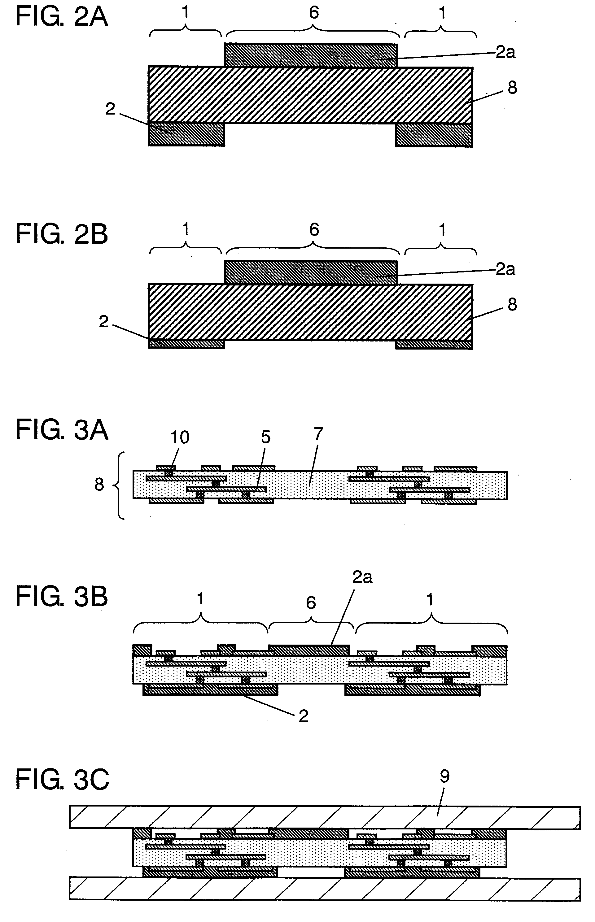
[0107]FIGS. 3A to 3C show major manufacturing steps of wiring board 8 of the present invention. FIG. 3A shows wiring board 8 configured with electrically insulating base 7, wiring pattern 5, and via 10. Aforementioned materials can be used for electrically insulating base 7. The drawings show the case of vias with IVH (inner via hole) structure in all layers, a so-called any-layer IVH. However, the present invention is not limited to this structure. A through-hole via structure and build-up board structure are also applicable. Via 10 is made of conductive paste filled in a hole. The use of incompressible base such as nonwoven aramid fabric base and glass epoxy base for electrically insulating base 7 achieves wiring board 8 with even denser structure.

[0108]Since nonwoven aramid board has lower elastic modulus and thus low board rigidity, compared to that of the glass epoxy board, the warp-correcting portion of the present invention can further effectively correct warping.

[0109]Next, ...

third exemplary embodiment

[0116]FIG. 4 show a semiconductor device on which a semiconductor is bare-chip mounted as an example of a component mounted on a wiring board of the present invention. FIG. 4A is a wiring board sheet of the present invention, illustrating, as an example, a four-layer board with the any-layer IVH structure. However, the structure of wiring board is not limited. Warping of the wiring board sheet can be reduced by forming warp-correcting portion 6. Warp-correcting portion 6 can be disposed at predetermined positions in response to the warping state of product portion 1, as already described.

[0117]Semiconductor chip 11 is mounted as an electronic component on product portion 1 of this wiring board sheet. FIG. 4B is a sectional view taken along H-H′ in FIG. 4A, and illustrates the mounted state of semiconductor chip 11. Wiring protection layer 2 is formed entirely over a face different from the face where the semiconductor chip is mounted on wiring board 8, and then solder ball 12 is pro...


PUM

PropertyMeasurementUnit
elastic modulusaaaaaaaaaa
thickaaaaaaaaaa
thickaaaaaaaaaa

Abstract

A wiring board which includes a product portion configured with at least one layer of electrically insulating base, a wiring pattern formed on the surface or inner portion of the electrically insulating base, and a wiring protection layer which is formed on the surface of the board and has an opening. Warping over the entire wiring board can be reduced since this wiring board has a warp-correcting portion warped in a direction different from that of the product portion.

Description

TECHNICAL FIELD[0001]The present invention relates to thin resin wiring boards, including rigid boards and flexible boards, and more particularly to wiring boards featuring curable solder resist and their manufacturing methods.BACKGROUND ART[0002]The density of components mounted on wiring boards is rapidly increasing in response to the further downsizing and advancement of electronic apparatuses. For mobile devices, in particular, there are growing demands for electronic components mounted on thinner wiring boards to occupy a lower profile.[0003]In response to these demands, a thinner electrically insulating base has been developed for the wiring boards used in these types of electronic apparatuses. For example, thinner boards but with the same number of layers are now feasible. A four-layer rigid board of 0.25 mm or thinner and multilayer flexible board about 0.1 mm thick have been put into practical use. For applications which conventionally require six to eight layers in multila...

Claims


Application Information

Patent Timeline
Patent Type & Authority Applications(United States)
IPC IPC(8): H05K1/11H05K1/00B05D5/12
CPCH01L21/563H01L23/49805H01L2224/73204H01L2224/32225H01L2224/16225H05K2203/1105H05K2203/0278H05K2201/2009H05K2201/09909H05K2201/09136H01L23/49816H01L23/49838H01L2224/16H01L2924/15311H01L2924/15331H01L2924/3511H05K1/0271H05K3/0052H01L2924/00H01L2224/05568H01L2224/05573H01L2924/00014H01L2224/05599
Inventor HIGASHITANI, HIDEKI
Owner PANASONIC CORP
Why Eureka
Try Eureka