Light Emitting Device and Backlight Unit Using the Same

a backlight unit and light emitting device technology, applied in the field of backlight units and light emitting devices using the same, can solve the problems of uneven coloration of light projected from optoelectronic devices, uneven surface imperfections, and uneven light emission, and achieve excellent adhesion, thin backlight units, and enhanced light take-out efficiency

Active Publication Date: 2009-05-28
NICHIA CORP
View PDF15 Cites 15 Cited by
  • Summary
  • Abstract
  • Description
  • Claims
  • Application Information

AI Technical Summary

Benefits of technology

[0014]The backlight unit of the present invention comprises the light emitting device and a light guide plate into which light from the light emitting device is incident. Thereby, a very thin backlight unit can be provided. When the light emitting device is fit into the light guide plate, light take-out efficiency can be enhanced since the light emitting device has a smooth surface and is excellent in adhesion with the light guide plate.
[0015]With the above-described constitution of the present invention, it is possible to enhance adhesion between the sealing member and the package. It is also possible to provide a light emitting device using a package having excellent light resistance.

Problems solved by technology

When polyphthalamide and glass fibers are mixed and formed, unevenness is formed on the surface of the jacket.
A conventional optoelectronics device using a jacket containing glass fibers mixed therein has a problem that glass fibers extrude from the surface of the jacket to cause so-called burrs since glass fibers are long.
There is also a problem that the jacket containing glass fibers mixed therein has an uneven surface and is therefore likely to cause wetting failure, and is insufficient in adhesion with a cover material, causing flaking.
As a result of flaking of the cover material, a reflective surface is formed between the space between the cover material and the jacket to cause uneven coloring of light projected from the optoelectronics device.

Method used


Image

  • Light Emitting Device and Backlight Unit Using the Same
  • Light Emitting Device and Backlight Unit Using the Same
  • Light Emitting Device and Backlight Unit Using the Same

Examples


example 1

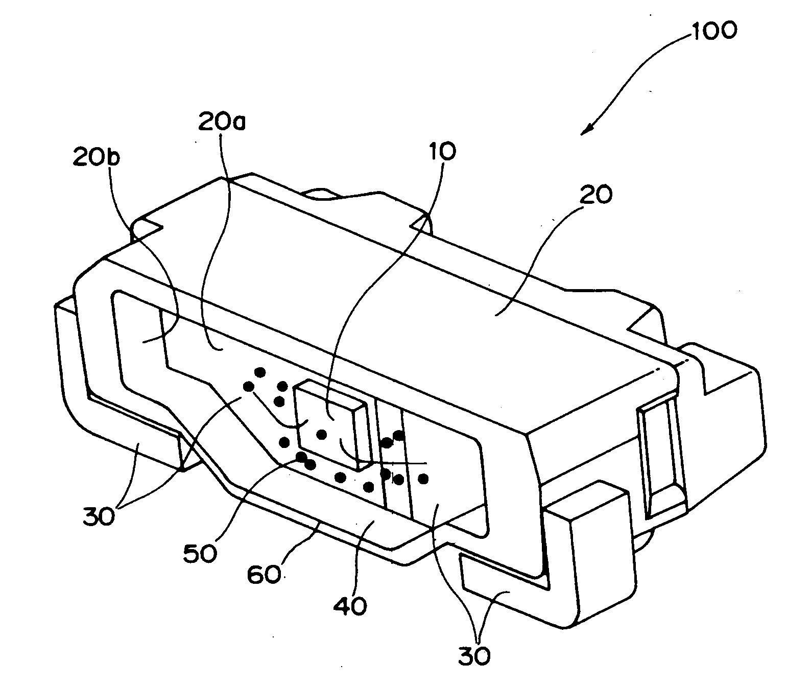
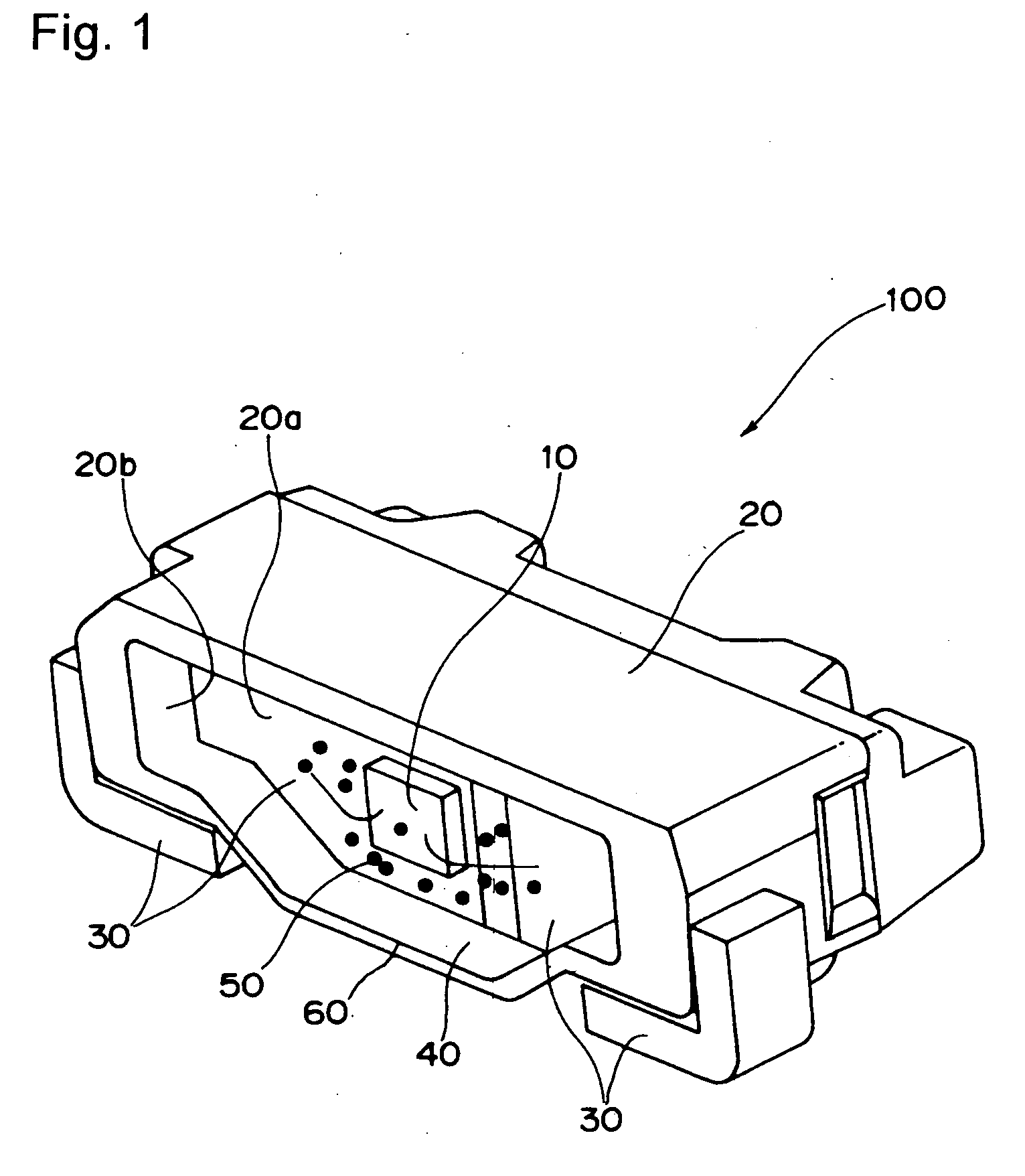
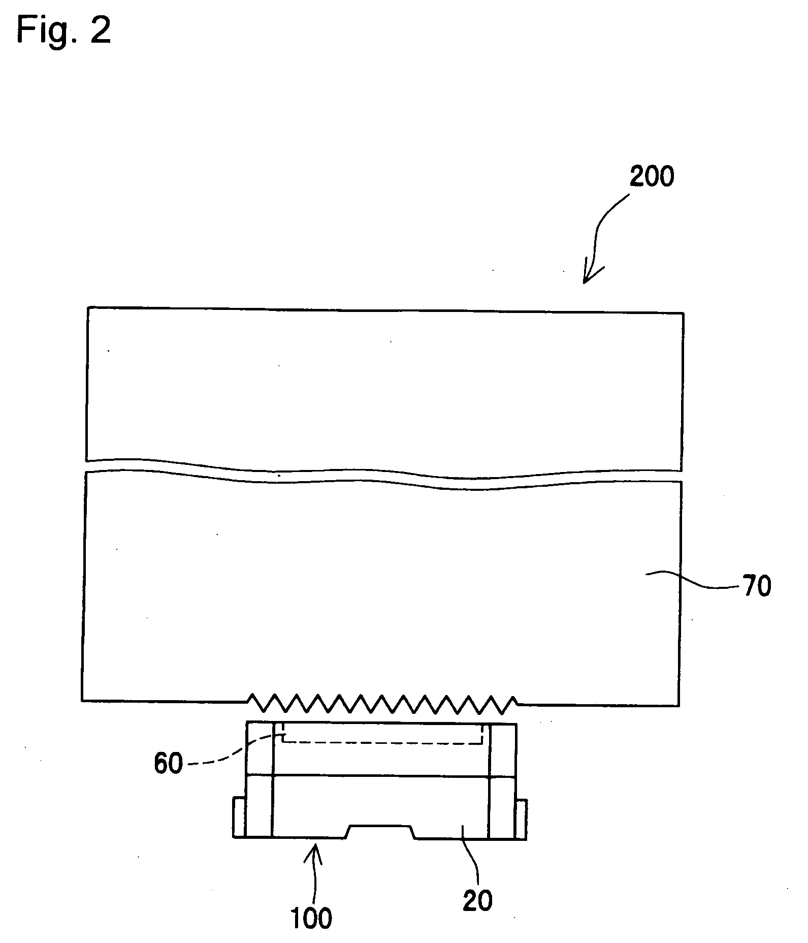
[0062]A light emitting device 100 in the form shown in FIG. 1 is produced. A package 20 means a side emitting light emitting device and does not show a strict structure of the package 20.

[0063]As the light emitting element 10, a light emitting element capable of emitting blue light having a peak emission wavelength at 460 nm is used. As the material of the sealing member 40, silicone (manufactured by Shin-Etsu Chemical Co., Ltd. under the trade name of KJR9032) is used. As the package 20, a package of a side emitting light emitting device (NSCW008 manufactured by Nichia Corporation) is used. The thickness of a side wall 20b of a recess 60 of the package 20 is from 70 to 80 μm.

[0064]The package 20 of Example 1 contains 20% by weight of wollastonite, 15% by weight of titanium oxide and 64% by weight of a semiaromatic polyamide. This semiaromatic polyamide contains 50 mol % of an aromatic monomer, and an amount of the amide group is 30 g or less in 100 g of the semiaromatic polyamide. ...

example 2

[0065]In Example 2, a light emitting device 100 is produced in the same manner as in Example 1, except that the material of the package 20 is changed. As the semiaromatic polyamide, polyphthalamide having a composition different from that in Example 1 is used.

example 3

[0066]In Example 3, a light emitting device 100 is produced in the same manner as in Example 1, except that the package 20 different from that in Example 1 is used. As the package 20, a package of a side emitting light emitting device (NSCW020 manufactured by Nichia Corporation) is used. The thickness of a side wall 20b of a recess 60 of the package 20 of Example 3 is from 70 to 80 μm. As the semiaromatic polyamide of Example 3, the same one as in Example 1 is used.


PUM

PropertyMeasurementUnit
thicknessaaaaaaaaaa
peak emission wavelengthaaaaaaaaaa
diameteraaaaaaaaaa

Abstract

An object of the present invention is to provide a light emitting device that shows high adhesion between a sealing member and a package member. A light emitting device 100 of the present invention comprises a package 20 with a recess 60 having a bottom face 20a and a side wall 20b, a light emitting element 10 mounted on the bottom face 20a of the recess 60 of the package 20, and a sealing member 40 filled in the recess 60 of the package 20, with which the light emitting element 10 is coated, wherein the package 20 contains, against the entire monomer component, from 5 to 70% by weight of potassium titanate fibers and/or wollastonite, from 10 to 50% by weight of titanium oxide, and from 15 to 85% by weight of a semiaromatic polyamide containing 20 mol % or more of an aromatic monomer, a part of the side wall 20b of the recess 60 of the package 20 has a thickness of 100 μm or less, and the sealing member 40 is made of silicone.

Description

BACKGROUND OF THE INVENTION[0001]1. Field of the Invention[0002]The present invention relates to a light emitting device that is used for lighting equipment, a display, a backlight of a cellular phone, an auxiliary light source for moving image lighting, and other common consumer light sources. More particularly, the present invention relates to a light emitting device in which a semiconductor light emitting element is mounted on a package and sealed with a silicone sealing member.[0003]2. Description of the Related Art[0004]A light emitting device using a light emitting element composed of a semiconductor is small-sized and is excellent in power efficiency, and also emits light of a vivid color. A light emitting element used has such a feature that it may not burn out because it is a semiconductor element, and is also excellent in initial drive characteristics and has strong resistance against vibration or repetition of turning a light on / off. The light emitting device using a ligh...

Claims


Application Information

Patent Timeline
Patent Type & Authority Applications(United States)
IPC IPC(8): H01L33/00H01L33/48H01L33/56
CPCH01L33/486H01L33/56H01L2224/48091H01L2924/3025H01L2924/00014H01L2924/00C08L77/00G02F1/1335G02F1/1339
Inventor KITANI, MOTOHISAICHIKAWA, HIROFUMITSUKIOKA, TOMOYAMIKI, TOMOHIDEKURAMOTO, MASAFUMI
Owner NICHIA CORP
Why Eureka
Try Eureka