Metal pattern and process for producing the same

a technology of metal patterns and metal parts, applied in the field of metal patterns, can solve the problems of increasing manufacturing costs, waste of materials, and waste of 90% or more of resist solutions in the resist application process, and achieve the effects of reducing manufacturing costs, reducing manufacturing costs, and increasing manufacturing costs

Inactive Publication Date: 2009-06-04
PANASONIC CORP
View PDF2 Cites 11 Cited by
  • Summary
  • Abstract
  • Description
  • Claims
  • Application Information

AI Technical Summary

Benefits of technology

[0025]To solve the above-described problems of the prior art, it is an object of the present invention to provide an accurate metal pattern without blurring, by causing specific molecules to enter interstices between specific molecules composing a monomolecular film so as to form a masking film, and to provide a method for producing the foregoing metal pattern.

Problems solved by technology

The photolithography method is very useful as a metal patterning method, but it has several problems.
The first problem is waste of materials, i.e., 90% or more of the resist solution is wasted in the resist application process.
The second problem arises in that a large amount of an organic solvent, which possibly is harmful to the environment, has to be used in the developing and removing processes, and this is unfavorable from the viewpoint of the environmental protection.
The third problem is in that in the case where various types of products are to be manufactured in small volumes, respectively, a costly photomask has to be produced for each of the product types, which increases the manufacturing costs.
Still further, the photolithography method involves many steps, and if a method involving a smaller number of steps is developed, it will leads to a decrease in the manufacturing costs.
Still further, since in the method employing the ink jet method, a liquid is jetted by using digital data prepared on computer so that a pattern is formed directly on a substrate, a costly photomask is unnecessary.
Further, since in the method employing the ink jet method, a liquid is jetted by using digital data prepared on computer so that a pattern is formed directly on a substrate, a costly photomask is unnecessary.
The monomolecular film, filled with molecules densely, does not allow the etching solution to permeate therethrough, and therefore, functions as a resist film for a metal.
However, at such a temperature, a normal substrate is denatured due to heat.
Particularly in circuit wiring, a decrease in the conductivity is a significant problem since it leads to deterioration of the device performance.
However, a stamp has to be prepared for each pattern, and hence, this method is not suitable for the manufacturing of a variety of products in small volumes.Patent Document 1: JP 2002-299833 APatent Document 2: JP 2002-324966 APatent Document 3: JP10(1998)-204350 APatent Document 4: JP 2002-13487 APatent Document 5: JP 3245410 BPatent Document 6: JP 2000-340928 ANon-Patent Document 1: Applied Physics Vol. 63, p.4, 1993Non-Patent Document 2: Synthetic Metals Vol. 115, p.

Method used


Image

  • Metal pattern and process for producing the same
  • Metal pattern and process for producing the same
  • Metal pattern and process for producing the same

Examples


example 1

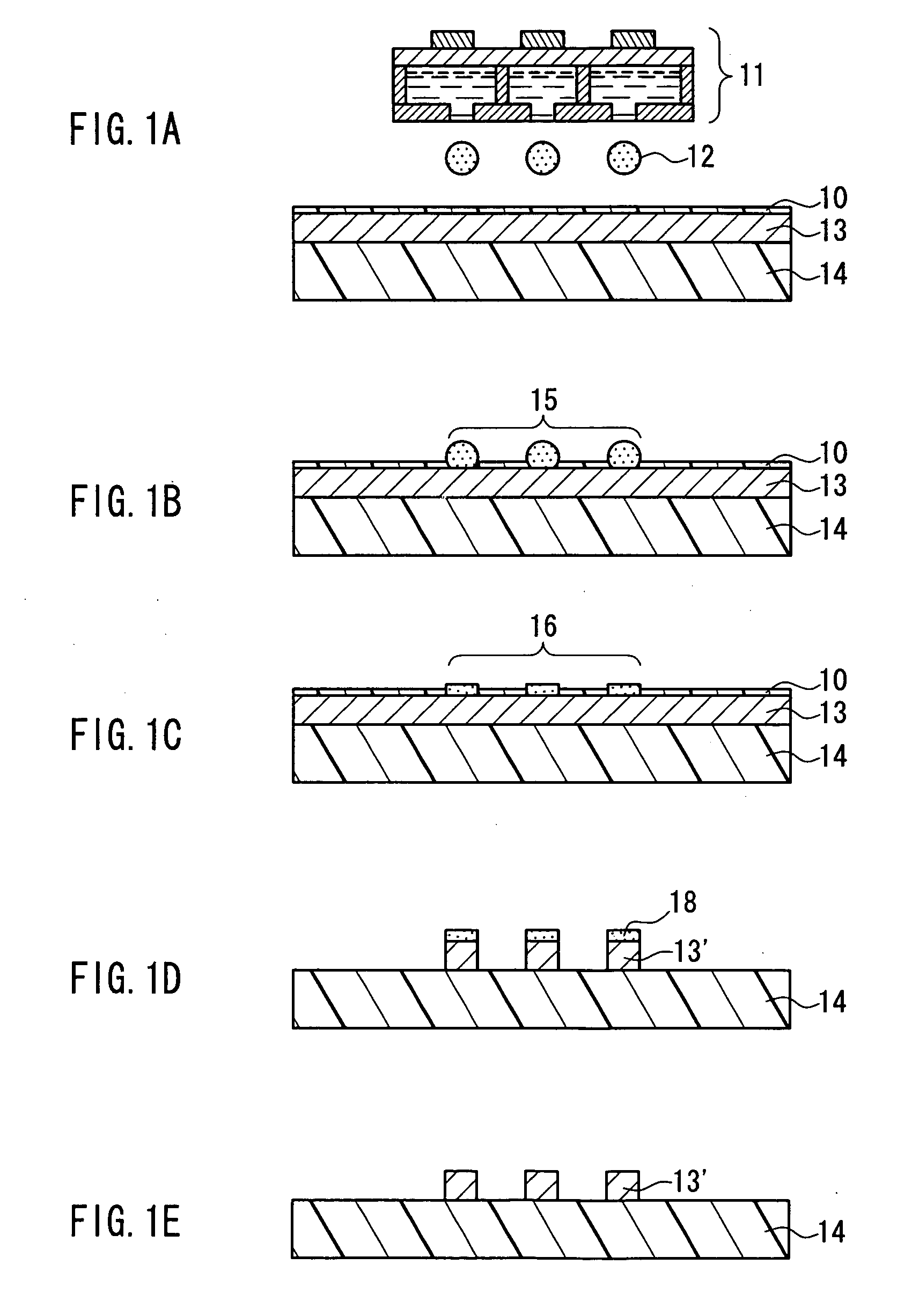
(1) Preparation of Substrate

[0093]A surface of a 4-inch silicon wafer was exposed to an ozone atmosphere at 110° C. so that organic matters on the surface were removed, and subsequently a 300 nm-thick copper film was formed on the surface by electron-beam evaporation.

(2) Formation of A Monomolecular Film Having Fluorinated Alkyl Chains

[0094]An ethanol solution in which CF3(CF2)7C2H4SH was dissolved at a concentration of 10−4 vol % was prepared. The silicon wafer with the copper film formed thereon was immersed in the foregoing solution for a predetermined time, and was removed therefrom. The silicon wafer then was washed with pure ethanol, and subsequently was washed with running pure water. The water repellency of a monomolecular film thus formed was evaluated by measuring a static contact angle of the film with respect to pure water.

(3) Preparation of Liquid To Be Jetted

[0095]An ethanol solution in which hexadecane thiol (CH3(CH2)15SH) was dissolved at a concentration of 0.1 vol %...

example 2

[0114]Copper patterning was carried out in the same manner as that of Example 1 except that each monomolecular film having fluorinated alkyl chains was formed by the following method.

(1) Formation of Monomolecular Film Having Fluorinated Alkyl Chains

[0115]After a silicon wafer was immersed for a predetermined time in a solution of a mixture of n-hexadecane and chloroform (volume ratio: 4:1) in which CF3(CF2)7C2H4SiCl3 was dissolved at a concentration of 10−4 vol %, the silicon wafer was washed with chloroform. The foregoing process was carried out in a glove box filled with dried nitrogen. Next, the silicon wafer was removed from the glove box, and was washed with running water for approximately 5 minutes.

(2) Result

[0116]The result is shown in Table 2 below. With immersion for 1 to 20 minutes, copper patterns were formed in the same manner as Example 1.

[0117]As a result of the immersion for 60 minutes, a maximum line width of 102 μm was obtained, which was close to a value of the id...

example 3

[0123]Copper patterning was carried out in the same manner as that of Example 1 except that each monomolecular film having fluorinated alkyl chains was formed by the following method.

(1) Formation of Monomolecular Film Having Fluorinated Alkyl Chains

[0124]After a silicon wafer was immersed for a predetermined time in an ethanol solution in which 0.1 vol % of CF3(CF2)7C2H4Si(OCH3)3, 1 vol % of water, and 0.01 vol % of hydrochloric acid were dissolved, the silicon wafer was washed with ethanol. Thereafter, the silicon wafer was washed with running pure water.

(2) Result

[0125]The result is shown in Table 3 below. With immersion for 30 to 120 minutes, copper patterns were formed in the same manner as Example 1.

[0126]As a result of the immersion for 240 minutes, a maximum line width of 102 μm was obtained, which was close to a value of the ideal pattern, but copper remained partially in a region onto which the solution was not jetted, not being removed by etching. It is supposed that this...


PUM

PropertyMeasurementUnit
temperatureaaaaaaaaaa
particle diameteraaaaaaaaaa

Abstract

A metal pattern of the present invention is a metal pattern (13′) formed on a surface of a substrate by etching, and a monomolecular film containing fluorinated alkyl chains (CF3(CF2)n—, where n represents an integer) is formed on a surface of a metal film composing the metal pattern (13′), and a masking film (18) is formed by penetration of a molecule having a mercapto group (—SH) or a disulfide (—SS—) group into interstices between molecules composing the monomolecular film. The metal pattern is produced by: forming a monomolecular film containing fluorinated alkyl chains (CF3(CF2)n—, where n represents an integer) on a surface of a metal film; forming a masking film by applying a solution in which a molecule having a mercapto group (—SH) or a disulfide (—SS—) group is dissolved over a surface of the monomolecular film so that the molecule having a mercapto group (—SH) or a disulfide (—SS—) group penetrates in interstices between molecules composing the monomolecular film; and etching the metal film by exposing the surface of the metal film to an etching solution so that a portion of the metal film in a region not covered with the masking film is removed.

Description

TECHNICAL FIELD[0001]The present invention relates to a metal pattern that can be formed by micromachining, and a method for producing the same.BACKGROUND ART[0002]Conventionally, a pattern of a metal is formed by photolithography. An outline of the photolithography technique is described as follows. A resist solution is applied by spin-coating over a substrate on which a metal film is formed, and drying at a low temperature is performed so that excess solution is removed. Next, a photomask is caused to adhere to the substrate, and is irradiated with ultraviolet radiation. By so doing, regions having been irradiated with light (hereinafter referred to as irradiated regions) and regions not having been irradiated with light (hereinafter referred to as non-irradiated regions) are formed on a surface of the resist film. The irradiated regions and the non-irradiated regions have different resistances with respect to a resist developer. Next, the substrate is exposed to the resist develo...

Claims


Application Information

Patent Timeline
Patent Type & Authority Applications(United States)
IPC IPC(8): B41N3/00C23F1/02C23F1/16C23F1/18C23F1/30C25D5/02H01L21/033H01L21/3213H01L51/00H05K3/06
CPCC23F1/02H05K2203/122C23F1/18C23F1/30C25D5/022H01L21/0332H01L21/0337H01L21/32139H01L51/0019H01L51/0022H05K3/061H05K2201/015H05K2201/0239H05K2203/013H05K2203/0582H05K2203/0585C23F1/16C23F1/14C23F1/40H10K71/236H10K71/611H05K3/125
Inventor NAKAGAWA, TOHRU
Owner PANASONIC CORP
Why Eureka
Try Eureka