Ferroelectric stacked-layer structure, field effect transistor, and ferroelectric capacitor and fabrication methods thereof

a technology of ferroelectric capacitors and stacked layers, which is applied in the direction of fixed capacitor details, natural mineral layered products, instruments, etc., can solve the problems of difficult to grow sto single crystals in a large diameter, difficult to use epitaxial growth methods, and difficult to grow sto single crystals in a large volume. , to achieve the effect of reducing the carrier trap level, excellent interface properties, and excellent electric characteristics

Inactive Publication Date: 2009-06-18
PANASONIC CORP
View PDF9 Cites 33 Cited by
  • Summary
  • Abstract
  • Description
  • Claims
  • Application Information

AI Technical Summary

Benefits of technology

[0026]According to the present invention, the second ferroelectric film, provided on the planarized first ferroelectric film, has a planar surface with no crystal defect. It is therefore possible to achieve a ferroelectric stacked-layer structure having excellent interface properties with reduced carrier trap level. It is also possible to achieve a field effect transistor or a ferroelectric capacitor which has excellent electric characteristics by using the above ferroelectric stacked-layer structure having excellent interface properties for a gate insulating film or a capacitor film.

Problems solved by technology

However, it is difficult to grow STO single crystals in a large diameter.
Hence, STO single crystals do not lend themselves to mass production.
It is therefore difficult to use an epitaxial growth method.

Method used


Image

  • Ferroelectric stacked-layer structure, field effect transistor, and ferroelectric capacitor and fabrication methods thereof
  • Ferroelectric stacked-layer structure, field effect transistor, and ferroelectric capacitor and fabrication methods thereof
  • Ferroelectric stacked-layer structure, field effect transistor, and ferroelectric capacitor and fabrication methods thereof

Examples


first embodiment

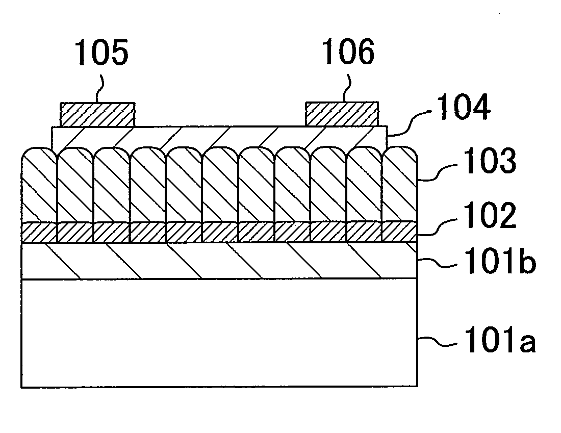
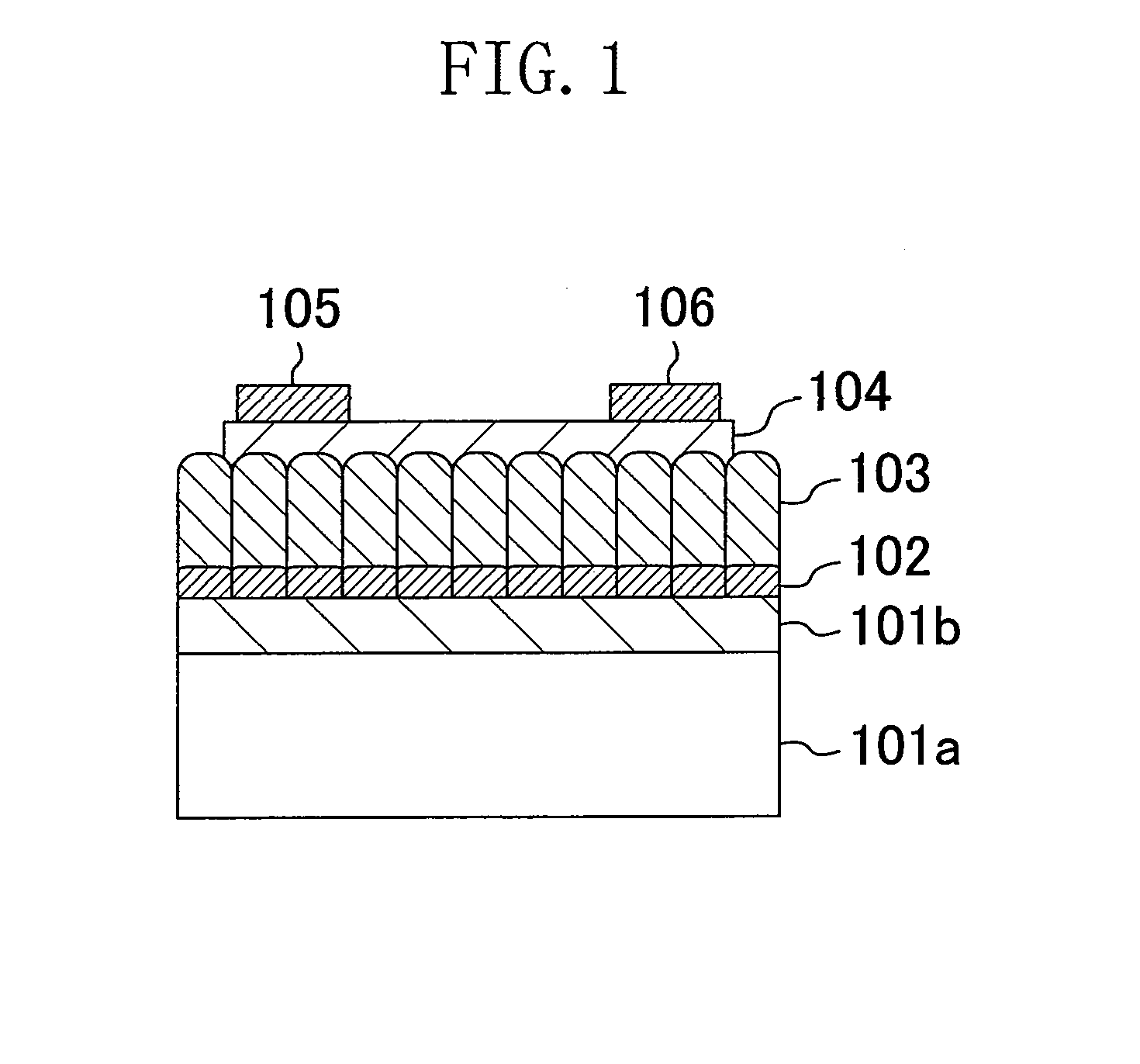
[0062]FIG. 6 is a schematic cross section of the structure of a field effect transistor according to the present invention.

[0063]As shown in FIG. 6, a field effect transistor according to the present embodiment includes a gate insulating film 3 composed of a ferroelectric stacked-layer structure, 3a and 3b. The basic structure of the field effect transistor is the same as that of the structure shown in FIG. 1.

[0064]The ferroelectric stacked-layer structure includes a first polycrystalline ferroelectric film 3a and a second thin ferroelectric film 3b formed on the first ferroelectric film 3a. The first ferroelectric film 3a has a planarized surface, and the second ferroelectric film 3b has the same crystalline structure as that of the first ferroelectric film 3a.

[0065]The concrete structure of the field effect transistor according to the present embodiment is hereinafter described.

[0066]As shown in FIG. 6, a silicon oxide film 1b is provided on a silicon substrate 1a. A gate electro...

second embodiment

[0089]FIG. 13 is a schematic cross section of the structure of a ferroelectric capacitor according to the present invention, wherein a capacitor film 13 is composed of a ferroelectric stacked-layer structure, 13a and 13b.

[0090]The ferroelectric stacked-layer structure is composed of a first polycrystalline ferroelectric film 13a and a second thin ferroelectric film 13b stacked on the first ferroelectric film 13a. The first ferroelectric film 13a has a planarized surface, and the second ferroelectric film 13b has the same crystalline structure as that of the first ferroelectric film 13a.

[0091]The concrete structure of the ferroelectric capacitor according to the present embodiment is hereinafter described. Elements of the ferroelectric capacitor other than a lower electrode 12 and an upper electrode 15 are basically the same as the elements of the field effect transistor shown in FIG. 6. The detailed description of the identical elements is omitted.

[0092]As shown in FIG. 13, a lowe...


PUM

PropertyMeasurementUnit
thicknessaaaaaaaaaa
surface roughnessaaaaaaaaaa
chargeaaaaaaaaaa

Abstract

A ferroelectric stacked-layer structure is fabricated by forming a first polycrystalline ferroelectric film on a polycrystalline or amorphous substrate, and after planarizing a surface of the first ferroelectric film, laminating on the first ferroelectric film a second thin ferroelectric film having the same crystalline structure as the first ferroelectric film. A field effect transistor or a ferroelectric capacitor includes the ferroelectric stacked-layer structure as a gate insulating film or a capacitor film.

Description

BACKGROUND OF THE INVENTION[0001]The present disclosure relates to a ferroelectric stacked-layer structure and a fabrication method of the same, and to a field effect transistor or a ferroelectric capacitor in which a ferroelectric stacked-layer structure is used for a gate insulating film or a capacitor film and a fabrication method of the same.[0002]Nonvolatile memories can be generally divided into two types: capacitor type and FET (Field Effect Transistor) type in which a gate insulating film is composed of a ferroelectric film.[0003]The structure of the capacitor type is similar to that of DRAM (Dynamic Random Access Memory), in which charge is stored in a ferroelectric capacitor and the state of data, 0 or 1, is distinguished by the polarization direction of the ferroelectric material. Since data stored is destroyed while being read, the data needs to be rewritten. Therefore, the polarization is reversed every time the data is read, which leads to polarization reversal fatigue...

Claims


Application Information

Patent Timeline
Patent Type & Authority Applications(United States)
IPC IPC(8): H01L29/78H01L21/04H01G4/06B32B9/00
CPCG11C11/22H01G4/1227H01G4/30Y10T428/26H01L29/6684H01L29/78391H01L28/56
Inventor TANAKA, HIROYUKIKATO, YOSHIHISAKANEKO, YUKIHIRO
Owner PANASONIC CORP
Why Eureka
Try Eureka