Under bump metallurgy structure of semiconductor device package

a semiconductor device and bump metallurgy technology, applied in the direction of semiconductor devices, semiconductor/solid-state device details, electrical devices, etc., can solve the problems of increasing ic chip processing speed and ic chip pin count, and presenting a constant and formidable challenge to consumers and related articles, and achieves better adhesion and enhanced adhesion strength

Inactive Publication Date: 2009-06-25
ADVANCED CHIP ENG TECH
View PDF3 Cites 16 Cited by
  • Summary
  • Abstract
  • Description
  • Claims
  • Application Information

AI Technical Summary

Benefits of technology

[0014]The structure further comprises a metal seed layer formed under the UBM structure. UBM include a lower layer made of copper-containing layer and an intermediate layer made of nickel-containing layer as barrier layer. An upper layer is made of Au-containing layer. It is preferably the lateral embedded portions of the UBM are longer than 30 μm, and it can be extended to near next solder pads, it also prefers to add the via holes inside the lateral embedded portions of

Problems solved by technology

With the trend moving to more and more features packed into decreasing product envelopes, utilizing ever smaller electronic components to improve upon size and feature densification a constant and formidable challenge is presented to manufacturers of consumer and related articles.
New improved technologies for achieving fine-pitch wire bonding structures cannot keep pac

Method used


Image

  • Under bump metallurgy structure of semiconductor device package
  • Under bump metallurgy structure of semiconductor device package
  • Under bump metallurgy structure of semiconductor device package

Examples


Embodiment Construction

[0022]The present invention discloses a under bump metallurgy structure of package and method of the same. It can apply to a wafer level package. Some sample embodiments of the invention will now be described in greater detail. Nevertheless, it should be recognized that the present invention can be practiced in a wide range of other embodiments besides those explicitly described, and the scope of the present invention is expressly not limited expect as specified in the accompanying claims.

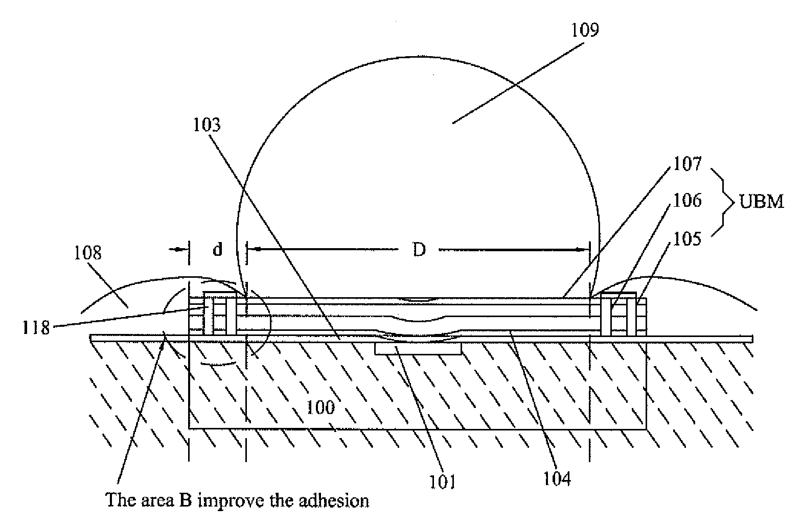
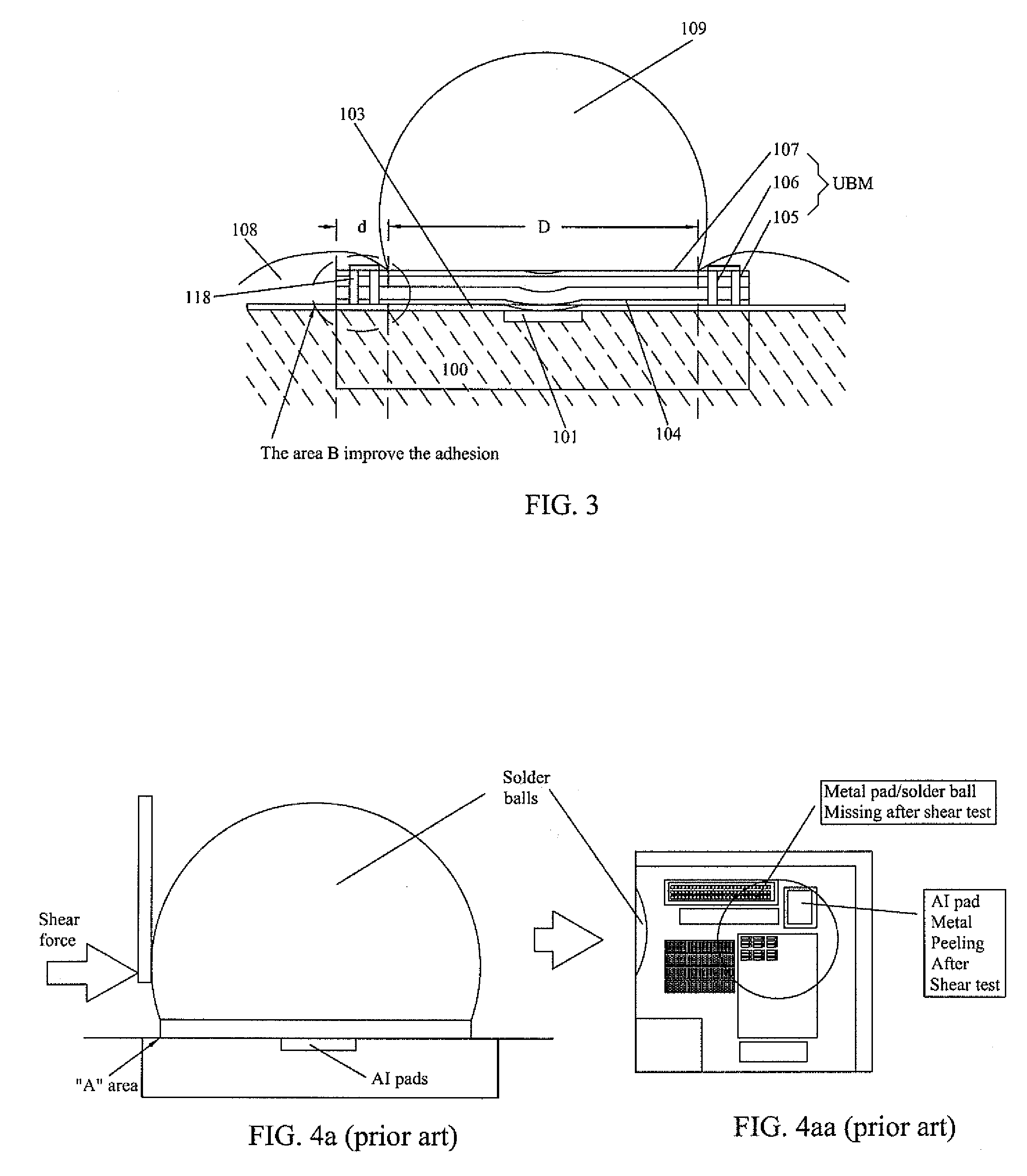
[0023]A new Under Bump Metallization (UBM) layer is disclosed herein which is especially suitable for use with a Wafer Level Chip Scale Package (WLCSP). The UBM dramatically improves package lifetime, and improve the peeling effect caused by the prior art structure.

[0024]The mechanical properties of the solder joint further improved by providing a larger area of contact between the material of the UBM and the dielectric material, thereby improving the integrity of the dielectric layer—UBM interface...


PUM


Abstract

The under bump metallization (UBM) structure of semiconductor device comprises a substrate having a bonding pad disposed on an active surface; a UBM adhered on the bonding pad, wherein the UBM includes lateral embedded portions and the size of the UBM is larger than the size of the bonding pad; a dielectric layer over the UBM having opening that is smaller than the size of the UBM so as to allow the lateral embedded portions being embedded into the dielectric layer with a desired dimension; and a conductive ball melted on the UBM within the opening defined by the dielectric layer.

Description

FIELD OF THE INVENTION[0001]This invention relates to a structure of package, and more particularly to a under bump metallurgy (UBM) structure of package and manufacturing of the same.BACKGROUND OF THE INVENTIONDescription of the Prior Art[0002]Typically in the electronic component world, integrated circuits (ICs) are fabricated on a semiconductor substrate, known as a chip, and most commonly are made of silicon. The silicon chip is typically assembled into a larger package which serves to provide effective enlargement of the distance or pitch between input / output contacts of the silicon making it suitable for attachment to a printed circuit board, and to protect the IC from mechanical and environmental damage. With the trend moving to more and more features packed into decreasing product envelopes, utilizing ever smaller electronic components to improve upon size and feature densification a constant and formidable challenge is presented to manufacturers of consumer and related arti...

Claims


Application Information

Patent Timeline
IPC IPC(8): H01L23/488
CPCH01L24/12H01L2224/13099H01L2924/10253H01L2224/16H01L2924/01013H01L2924/01022H01L2924/01029H01L2924/01073H01L2924/01074H01L2924/01078H01L2924/01079H01L2924/01082H01L2924/01322H01L2924/04953H01L2924/14H01L2924/01005H01L2924/01006H01L2924/01024H01L2924/01033H01L2924/01047H01L2924/00H01L2924/15788H01L2224/05027H01L2224/05022H01L2224/05001H01L2224/05572H01L2224/05124H01L2224/056H01L24/05H01L2224/05576H01L2224/02125H01L2224/02165H01L2224/02126H01L24/03H01L24/13H01L2924/00014
Inventor YANG, WEN-KUNYANG, CHIN-LUNG
Owner ADVANCED CHIP ENG TECH
Why Eureka
Try Eureka