Radio frequency IC device

a radio frequency ic and integrated circuit technology, applied in the structure of radiating elements, loop antennas with ferromagnetic cores, instruments, etc., can solve the problems of disadvantageous degradation of radiation characteristics of antennas, variations in loop coil inductance, etc., to prevent variations in radiation characteristics

Active Publication Date: 2009-06-25
MURATA MFG CO LTD
View PDF6 Cites 142 Cited by
  • Summary
  • Abstract
  • Description
  • Claims
  • Application Information

AI Technical Summary

Benefits of technology

[0006]In order to overcome the problems described above, preferred embodiments of the present invention provide a radio frequency IC device that is not susceptible to being affected by a usage environment, that can prevent variations in radiation characteristics, and that can be used in a wide frequency band.
[0008]In the radio frequency IC device according to a preferred embodiment of the present invention, a resonance frequency of a signal is set in the feeder circuit provided in the feeder circuit substrate. Thus, the radio frequency IC device normally operates when being attached to various articles, variations in radiation characteristic are prevented, and there is no need to change the design of the radiating plate for individual articles. Particularly, the at least two inductance elements provided in the feeder circuit substrate are wound in opposite directions, and thus magnetic fields generated by the inductance elements are canceled out, a Q value becomes small with no steepness in resonance characteristic, and thus a wideband characteristic can be obtained near the resonance frequency. Also, the directions of the magnetic fields are opposite of one another. That is, when one of the magnetic fields is directed upward, the other is directed downward. This corresponds to positive and negative of an AC supply, enabling almost 100% energy transmission to the radiating plate via magnetic field energy.
[0012]The feeder circuit substrate may include a laminate and the inside or surface of a bottom layer of the laminate may be provided with flat electrodes, the size thereof being the about the same as, or smaller than that of an outer shape of the at least two inductance elements when the feeder circuit substrate is viewed in a perspective plan view. By providing the flat electrodes, variations in coupling between the feeder circuit and the radiating plate can be minimized.
[0017]A portion of the at least two inductance elements may be exposed on a side surface of the feeder circuit substrate and the exposed portion may function also as a radiating plate. The portion of the inductance elements electromagnetically couples to the radiating plate on the side surface of the feeder circuit substrate, so that the radiation characteristic is enhanced.
[0018]The feeder circuit substrate may be a multilayer substrate made of, for example, ceramic or resin, or may be a flexible substrate. Particularly, by providing the inductance elements constituting the feeder circuit in the substrate, the feeder circuit is not susceptible to being affected by the outside of the substrate, so that variations in radiation characteristic can be prevented.

Problems solved by technology

This configuration has a disadvantage of causing variations in inductance of the loop coil and in characteristics of the matching circuit depending on the permittivity of the article to which the radio frequency tag is attached or the circumstances of the article.
These variations cause transmission loss of signals between the IC chip and the antenna, resulting in disadvantageous degradation of radiation characteristics of the antenna.
The antenna needs to be designed in accordance with the permittivity and other characteristics of the article to which the antenna is to be attached, which is very inconvenient.

Method used


Image

  • Radio frequency IC device
  • Radio frequency IC device
  • Radio frequency IC device

Examples


first preferred embodiment

FIGS. 1 to 4

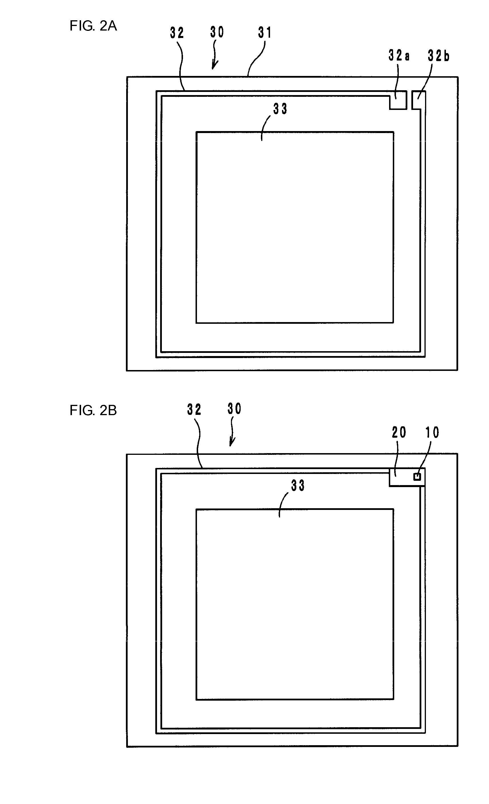
[0053]A radio frequency IC device according to a first preferred embodiment includes a radio frequency IC chip 10 arranged to process transmission / reception signals of predetermined frequencies and a feeder circuit substrate 20 on which the radio frequency IC chip 10 is mounted illustrated in FIG. 3, and also includes a radiating substrate 30 illustrated in FIG. 2A or FIG. 2B.

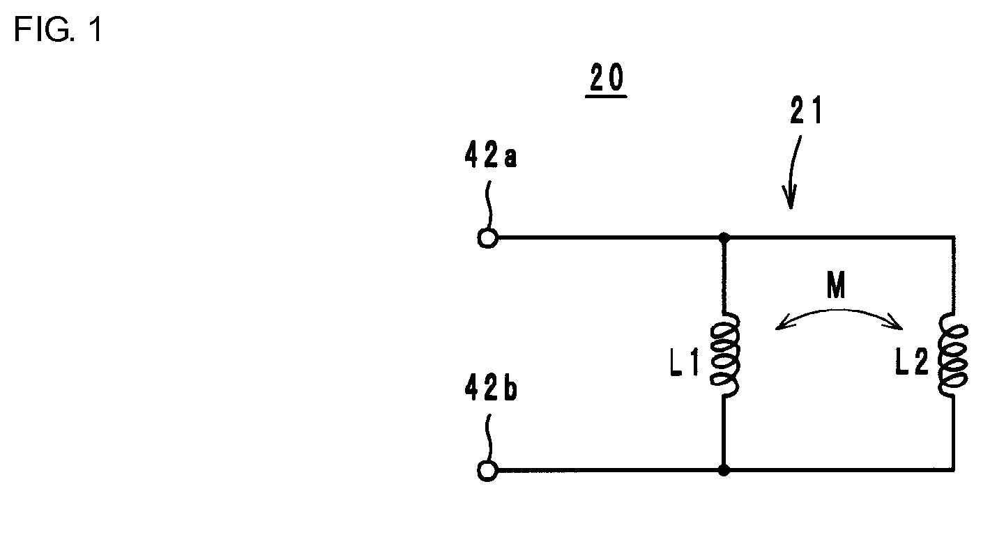
[0054]As illustrated in an equivalent circuit diagram in FIG. 1, the feeder circuit substrate 20 includes a feeder circuit 21 (the details are described below with reference to FIG. 4) having a resonance circuit and a matching circuit including inductance elements L1 and L2, which have inductance values that are different from each other and which magnetically couple to each other in opposite phases (indicated by mutual inductance M).

[0055]The radio frequency IC chip 10 includes, for example, a clock circuit, a logic circuit, a memory circuit, and so on, stores necessary information, and is provided...

second preferred embodiment

FIG. 5

[0070]A radio frequency IC device according to a second preferred embodiment preferably has basically the same configuration as that of the first preferred embodiment. As illustrated in FIG. 5, the difference between the first and second preferred embodiments is that flat electrodes 49a and 49b are provided on the rear surface of a sheet 41i in the bottom layer of the feeder circuit substrate 20. The size of the flat electrodes 49a and 49b preferably is the approximately the same as or smaller than that of the outer shape of the inductance elements L1 and L2, when the feeder circuit substrate 20 is viewed in a perspective plan view.

[0071]Via-hole conductors are placed at the end portions 46a-2 and 46b-2 of the wiring electrodes 46a and 46b forming the inductance elements L1 and L2. Those via-hole conductors connect to the feeder terminal electrodes 42a and 42b and also connect to the flat electrodes 49a and 49b via via-hole conductors 48c and 48d provided on the sheet 41i. By ...

third preferred embodiment

FIGS. 6 to 8

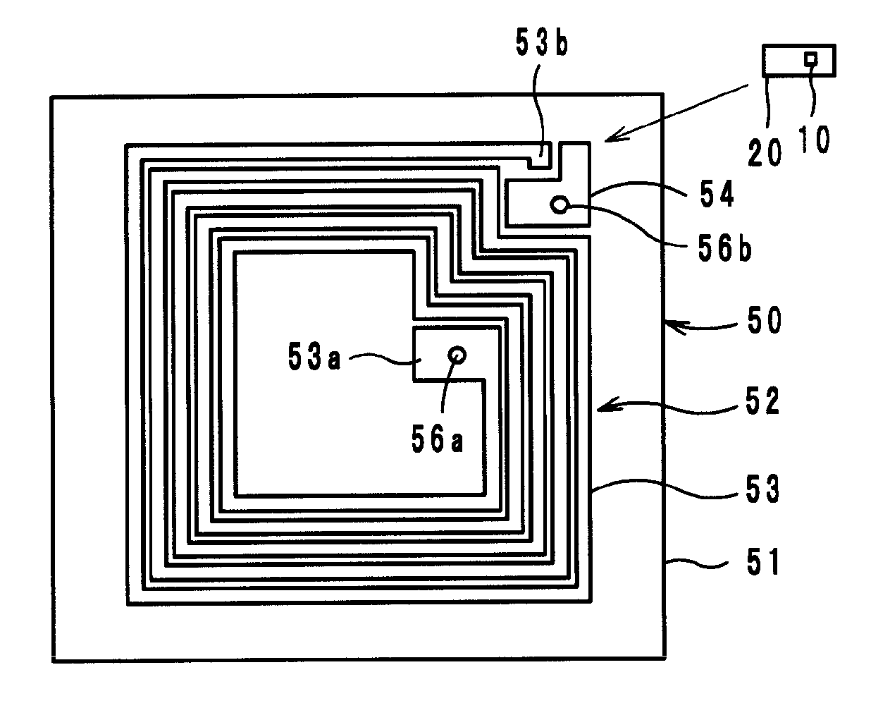
[0073]In a radio frequency IC device according to a third preferred embodiment, as illustrated in FIG. 7A, the feeder circuit substrate 20 on which the radio frequency IC chip 10 is mounted is bonded to an end portion 53b of an electrode 53 and an electrode 54 placed on a front surface of a radiating substrate 50 by an adhesive. The radio frequency IC chip 10 preferably has substantially the same configuration as that of the first preferred embodiment.

[0074]In the radiating substrate 50, the spiral electrode 53 and the electrode 54 defining a radiating plate 52 are placed on the front surface of a flexible resin film substrate 51, as illustrated in FIG. 7A, and a spiral electrode 55 defining the radiating plate 52 is placed on the rear surface thereof, as illustrated in FIG. 7B.

[0075]An end portion 53a of the electrode 53 electrically connects to an end portion 55a of the electrode 55 via a via-hole conductor 56a, and an end portion 55b of the electrode 55 electrically c...


PUM


Abstract

A radio frequency IC device includes a radio frequency IC chip, a feeder circuit substrate, and a radiating plate. The feeder circuit substrate includes a feeder circuit that electrically connects to the radio IC chip and that includes a resonance circuit and / or a matching circuit including inductance elements. The feeder circuit substrate is bonded to the radiating plate, which radiates a transmission signal supplied from the feeder circuit and supplies a received signal to the feeder circuit. The inductance elements are arranged in spiral patterns wound in opposite directions and couple to each other in opposite phases. The radio frequency IC device is able to obtain a radio frequency IC device that is not susceptible to being affected by a usage environment, minimizes variations in radiation characteristics, and can be used in a wide frequency band.

Description

BACKGROUND OF THE INVENTION[0001]1. Field of the Invention[0002]The present invention relates to a radio frequency IC (integrated circuit) device. More particularly, the present invention relates to a radio frequency IC device used in a RFID (radio frequency identification) system.[0003]2. Description of the Related Art[0004]Previous RFID systems have been developed as a system to manage articles. In this RFID system, a reader / writer generating an induction field and a radio frequency tag (also called a radio frequency IC device) that is attached to an article and that stores predetermined information communicate with each other in a non-contact manner to transmit information. As a radio frequency tag used in this type of RFID system, Japanese Unexamined Patent Application Publication No. 2006-80367 suggests a radio frequency tag including an antenna and a matching circuit placed on a flexible substrate and an IC chip electrically continuous to the antenna and the matching circuit. ...

Claims


Application Information

Patent Timeline
Patent Type & Authority Applications(United States)
IPC IPC(8): H01Q7/06H01Q11/12
CPCG06K19/07749H01Q1/2225H01F2017/002G06K19/077H05K1/02
Inventor KATO, NOBORUSASAKI, JUN
Owner MURATA MFG CO LTD
Why Eureka
Try Eureka