Electrostatic chuck and method of forming

a technology of electrostatic chuck and chuck, which is applied in the direction of liquid surface applicators, coatings, pretreated surfaces, etc., can solve the problems of low pressure in the chamber during semiconductor manufacturing processes, and affecting the quality of semiconductor products

Inactive Publication Date: 2009-06-25
SAINT GOBAIN CERAMICS & PLASTICS INC
View PDF14 Cites 17 Cited by
  • Summary
  • Abstract
  • Description
  • Claims
  • Application Information

AI Technical Summary

Problems solved by technology

Mechanical chucks have a disadvantage in that they often cause distortion of workpieces due to non-uniform forces being applied to the wafers.
Thus, wafers are often chipped or otherwise damaged, resulting in a lower yield.
In this respect, pressures in the chamber during semiconductor manufacturing processes tend to be low, and sufficient force cannot always be applied.
This shift to processing of larger workpieces, generally within high temperature and corrosive processing environments, places further demands on ESCs used during processing.

Method used


Image

  • Electrostatic chuck and method of forming
  • Electrostatic chuck and method of forming
  • Electrostatic chuck and method of forming

Examples


example 1

Comparative Samples, No Infiltration

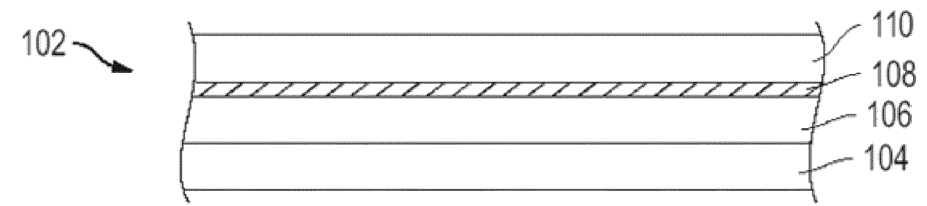
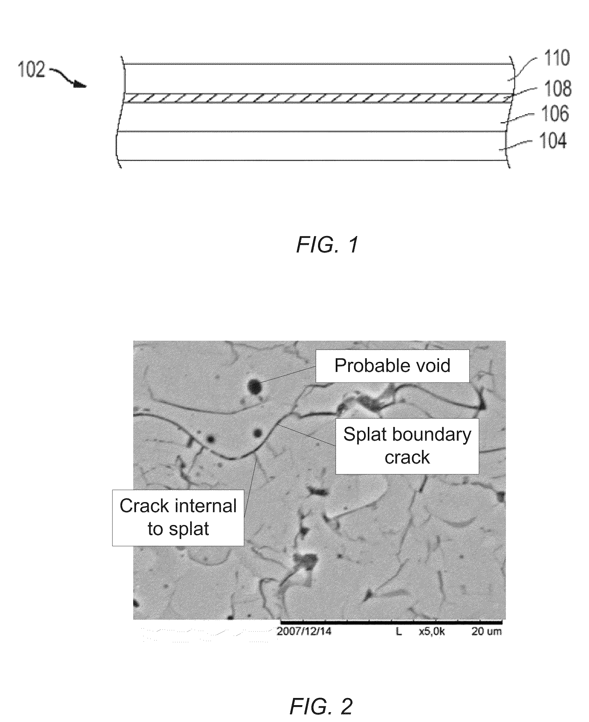
[0053]Four 6061 aluminum squares 4 cm on a side were grit blasted, plasma sprayed with aluminum oxide to a thickness of about 500 um to provide a porosity about 5%, and then plasma sprayed with tungsten on top to a thickness of about 50 um.

[0054]The samples were tested by applying a steadily increasing DC voltage between the tungsten and the base aluminum and monitoring current. Breakdown was deemed to occur when the current exceeded 2 mA.

TABLE 1Comparative SampleBreakdown voltage (kV)H2.5K10.3N4.7O2.1

[0055]The breakdown voltage varies, with a mean value of only 4.9 kV

example 2

Samples with Infiltration

[0056]Three samples were prepared as for example 1, but with the following addition. HL-126 acrylate monomer (obtained from Permabond LLC of Pottstown, Pa.) was painted onto the surface after spraying. Generous amounts were applied, so that the surface looked well wetted even after a minute or so was allowed for the liquid to soak into the pores. The samples were placed into a vacuum oven and several cycles of evacuation followed by backfill with argon were conducted. This served two purposes: the HL-126 was driven further into the pores and oxygen (which inhibits the cure of the monomer) was removed from the oven.

[0057]Samples were cured for about 2 hours at 120° C. They were then removed from the oven and an area over the tungsten was ground clean so that electrical contact could be established to the tungsten. The samples were then tested as in Example 1, with a maximum applied voltage of 10 kV.

[0058]In no case did breakdown occur, indicating the average ...

example 3

Additional Characterization

[0059]An important attribute of the infiltration process is that infiltrant not be removed by plasma gases. It was found unexpectedly that the infiltrant stays intact for a long time under etch conditions.

[0060]A set of coupons was plasma sprayed with yttrium oxide to a thickness of 100 um using a process that produces 4-5% porosity. They were infiltrated with HL-126 as described in Example 2 above.

[0061]The coupons were etched in a March PM-600 plasma asher (March Plasma Systems Inc., Concord, Calif.), with oxygen at 300W, 250 millitorr for extended times. The amount of infiltrant was determined by monitoring its fluorescence intensity.

[0062]FIG. 5 shows that, after a short initial transient (corresponding to removal of HL-126 from the surface), the infiltrant remains in the pores of the coating for an extended period of time.

[0063]The unexpected retention of infiltrant is not believed to be due to material properties of the infiltrant (which etches relat...


PUM

PropertyMeasurementUnit
pore sizeaaaaaaaaaa
dielectric constantaaaaaaaaaa
surface areaaaaaaaaaaa

Abstract

An electrostatic chuck includes an insulating layer, a conductive layer overlying the insulating layer, a dielectric layer overlying the conductive layer, the dielectric layer having pores forming interconnected porosity, and a cured polymer infiltrant residing in the pores of the dielectric layer.

Description

CROSS-REFERENCE TO RELATED APPLICATION(S)[0001]The present application claims priority from U.S. Provisional Patent Application No. 61 / 015,604, filed Dec. 20, 2007, entitled “Electrostatic Chuck and Method of Forming,” naming inventors Marc Abouaf, Stephen W. Into and Matthew A. Simpson, which application is incorporated by reference herein in its entirety.BACKGROUND[0002]1. Field of the Disclosure[0003]This disclosure is directed to an electrostatic chuck (ESC) and is particularly directed to electrostatic chucks for use in processing of flat panel displays.[0004]2. Description of the Related Art[0005]Chucks are used to support and hold wafers and substrates in place within high temperature and corrosive processing chambers such as those used for chemical vapor deposition, physical vapor deposition, or etching. Several main types of chucks have been developed. Mechanical chucks stabilize wafers on a supporting surface by using mechanical holders. Mechanical chucks have a disadvanta...

Claims


Application Information

Patent Timeline
Patent Type & Authority Applications(United States)
IPC IPC(8): H01L21/683B05D3/02
CPCH02N13/00
Inventor ABOUAF, MARCINTO, STEPHEN W.SIMPSON, MATTHEW A.
Owner SAINT GOBAIN CERAMICS & PLASTICS INC
Why Eureka
Try Eureka