Method for fabricating semiconductor device

a manufacturing method and semiconductor technology, applied in the direction of manufacturing tools, fine working devices, electric devices, etc., can solve the problem of the size of the semiconductor chips to be singulated from the semiconductor wafers becoming smaller, and achieve the effect of improving the manufacturing yield and decreasing the manufacturing yield

Active Publication Date: 2009-06-25
RENESAS ELECTRONICS CORP
View PDF2 Cites 126 Cited by
  • Summary
  • Abstract
  • Description
  • Claims
  • Application Information

AI Technical Summary

Benefits of technology

[0011]However, a size of the semiconductor chips to be singulated from the semiconductor wafer has become smaller. Accordingly, intervals between the dicing lines formed on the semiconductor wafer have become narrower. For this reason, a size of the scraps formed by dicing becomes smaller. Particularly, a semiconductor chip for use as a driver of a liquid-crystal display device has, for example, the rectangular shape, and the intervals between the dicing lines formed in a short-side direction of the rectangle becomes narrower.
[0012]As the scraps formed through dicing becomes smaller, an adhesive area to the dicing tape becomes smaller, so th

Problems solved by technology

However, a size of the semiconductor chips to be singu

Method used


Image

  • Method for fabricating semiconductor device
  • Method for fabricating semiconductor device
  • Method for fabricating semiconductor device

Examples


first embodiment

[0078]In a first embodiment, a method of manufacturing a Liquid Crystal Display (LCD) driver (semiconductor device) for use in a liquid-crystal display apparatus is described.

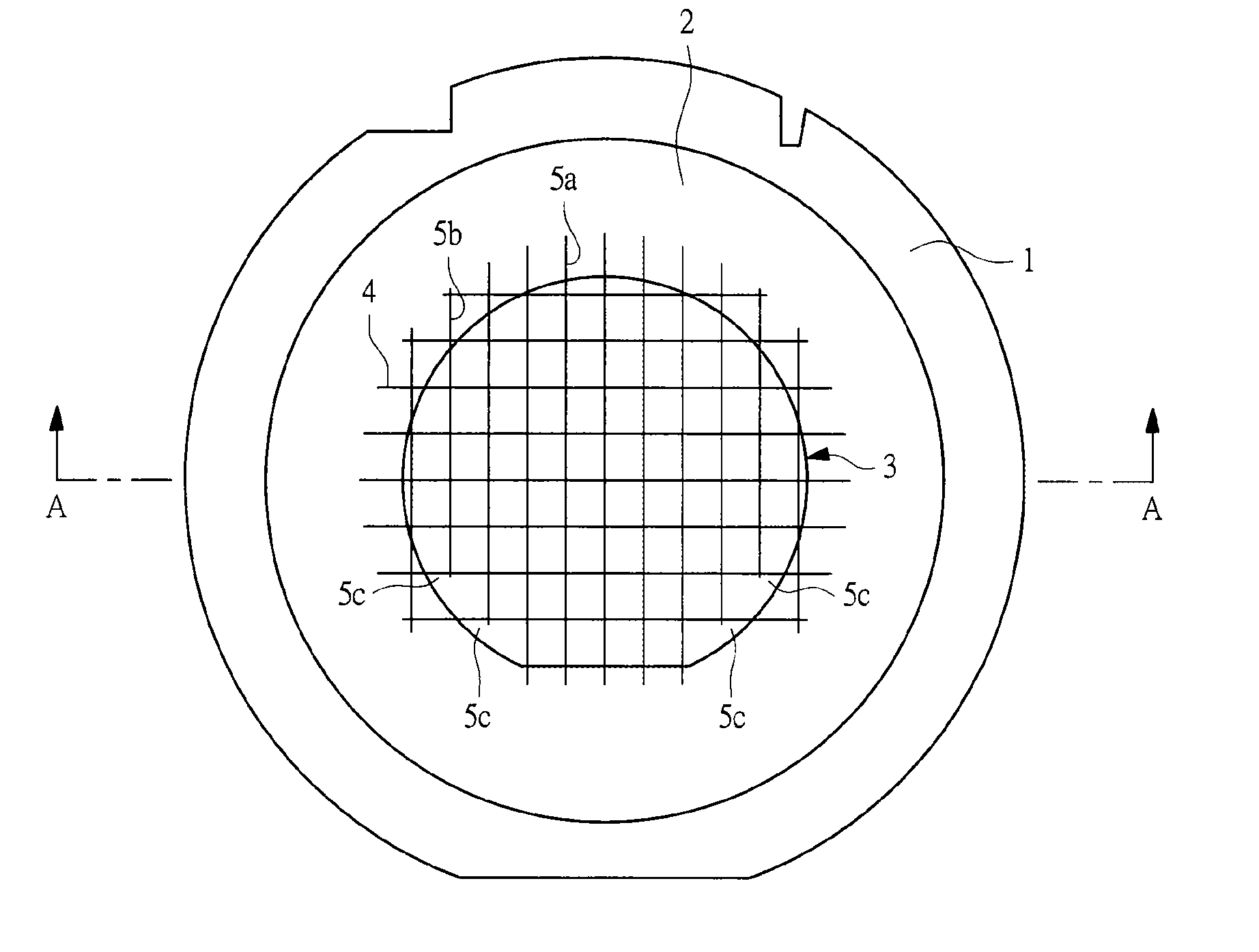
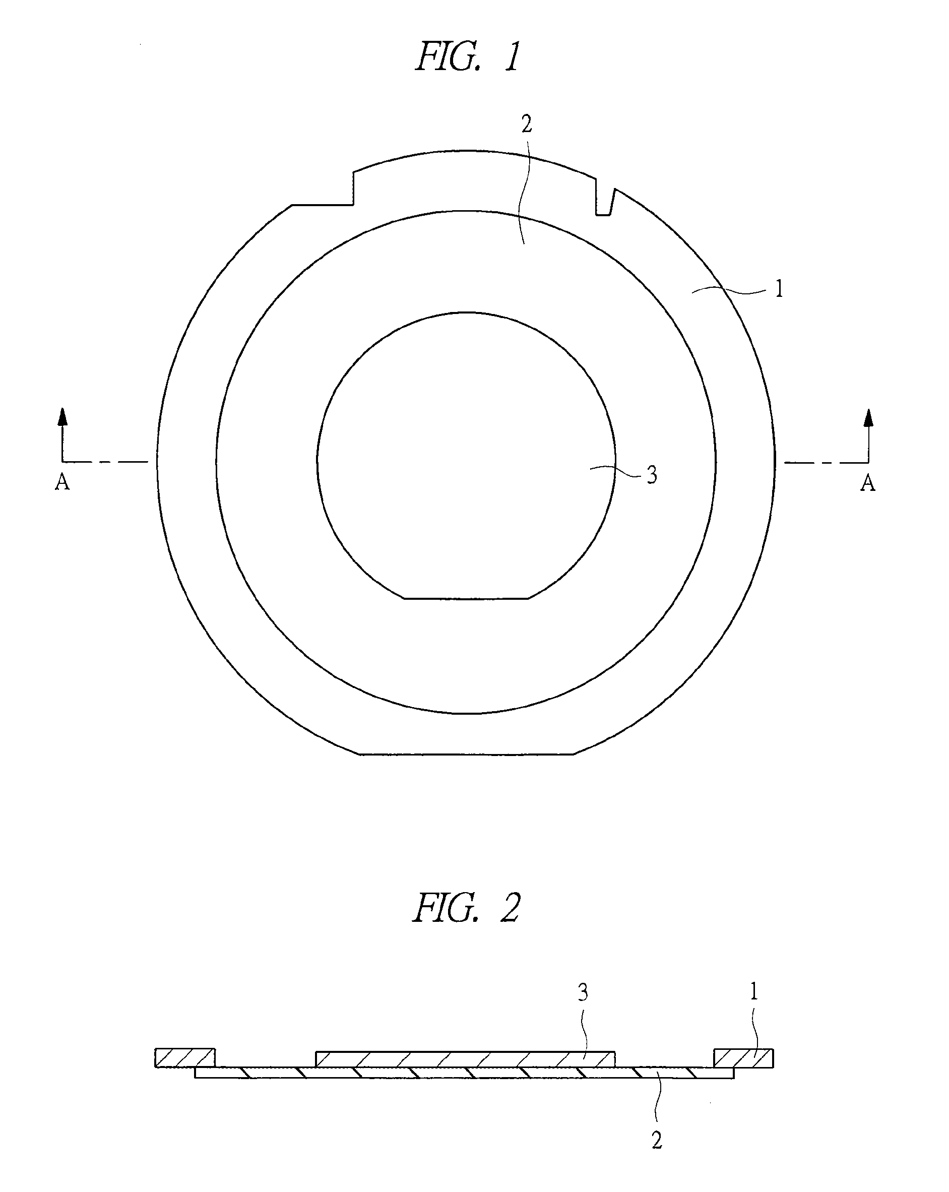
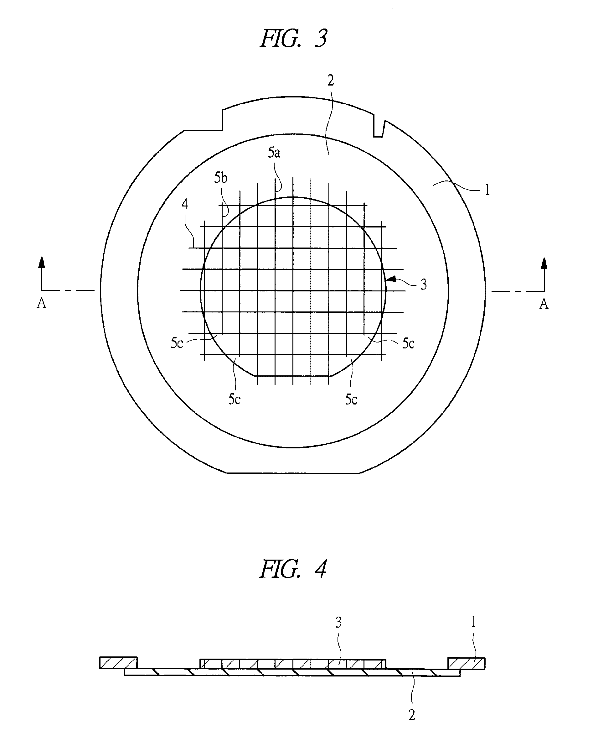
[0079]First, on a chip area of a semiconductor wafer with a substantially disk shape, a circuit element, such as Metal Insulator Semiconductor Field Effect Transistor (MISFET), is formed by using a well-known technology. Then, on an upper layer of the MISFET formed on the semiconductor wafer, a multilayer interconnection is formed. The multilayer interconnection is formed of, for example, metal wiring made of, for example, an aluminum film or an aluminum-alloy film with aluminum as a base metal, through an inter-layer insulating film composed of, for example, a silicon oxide film. Also, part or approximately all of layers forming the multilayer interconnections may be formed of copper films or films with copper as a base metal (damascene interconnection). Then, on the multilayer interconnection, a bump electrod...

second embodiment

[0139]In the first embodiment, the example has been described in which the dicing line group in the vertical direction and the dicing line group in the horizontal direction are both formed through the step-cutting. In a second embodiment, an example is described in which either one of the dicing line groups in the vertical or horizontal directions (second dicing line group) is formed through the single-cutting, while the other dicing line group (first dicing line group) is formed through the step-cutting.

[0140]FIG. 42 is a plan view showing the semiconductor wafer 3 to which dicing according to the second embodiment is performed. As shown in FIG. 42, semiconductor chips are for use in an LCD driver, and it can be seen that conforming chip area has a rectangular shape.

[0141]FIG. 43 is an enlarged plan view of a vicinity of the outer periphery 14 of the semiconductor wafer 3, and a plan view of an element formation surface (front surface) of the semiconductor wafer 3. FIG. 44 is an en...


PUM


Abstract

An object is to provide a technology capable of improving a manufacturing yield of semiconductor devices by preventing scattering of irregular-shaped scraps formed at the time of dicing. To achieve the above object, for dicing lines, by which an irregular-shaped outer periphery may possibly be cut off, among a plurality of dicing lines, formation of the dicing lines starts from an outside of a semiconductor wafer, and after the semiconductor wafer is cut off partway, formation of the dicing lines is ended before reaching the irregular-shaped outer periphery formed on a outer periphery of the semiconductor wafer. For other dicing lines, formation of the dicing lines starts from the outside of the semiconductor wafer, and after the semiconductor wafer is cut off, is ended outside the semiconductor wafer.

Description

TECHNICAL FIELD[0001]The present invention relates to a technology of manufacturing semiconductor devices, and more particularly, to a technology effective in being applied to a dicing process for singulating a semiconductor wafer into a plurality of semiconductor chips.BACKGROUND ART[0002]Japanese Patent Application Laid-open Publication No. 9-1542 (Patent Document 1) discloses a technology in which, in a cutting process for cutting a thin-plate material such as a semiconductor wafer into a plurality of members with a specified dimension, damages of a blade and the thin-plate material which are caused when scraps existing on a periphery of the thin-plate material are scattered and hit the blade and the thin-plate material are avoided. Specifically, a cutting stroke (cutting area) along the semiconductor wafer is set to be shorter than the entire length of a scribe-line, thereby leaving an uncut part on the periphery of the semiconductor wafer.[0003]Japanese Patent Application Laid-...

Claims


Application Information

Patent Timeline
IPC IPC(8): H01L21/78
CPCB28D5/022H01L21/78H01L21/67051
Inventor YUI, HAJIMEMURAMATSU, HISASHI
Owner RENESAS ELECTRONICS CORP
Why Eureka
Try Eureka