Reduced mask configuration for power mosfets with electrostatic discharge (ESD) circuit protection

a technology of circuit protection and mask configuration, which is applied in the direction of semiconductor devices, semiconductor/solid-state device details, diodes, etc., can solve the problems of degrading performance, complicated processing steps, and limitations of conventional layout for manufacturing semiconductor power devices with protection circuits against electrostatic discharge (esd). the effect of simplifying manufacturing process and improving semiconductor power device breakdown

Active Publication Date: 2009-07-02
ALPHA & OMEGA SEMICON LTD
View PDF11 Cites 28 Cited by
  • Summary
  • Abstract
  • Description
  • Claims
  • Application Information

AI Technical Summary

Benefits of technology

[0007]It is therefore an aspect of the present invention to provide a new and improved layout of an ESD protection circuit on a semiconductor power device by forming the ESD protection circuits in the termination area with guard ring surrounding the ESD structure to improve the semiconductor power device breakdown. It is further another aspect of the present invention to provide a new and improved layout of an ESD protection circuit on a semiconductor power device by forming the ESD protection circuits in the termination area with a different layout and layer structure by applying an ESD polysilicon layer to function also as a body block mask to achieve a simplified manufacturing process by removing a body mask requirement. By removing the requirement of using a body block mask, the manufacturing processes are simplified and the production cost is decreased while the production yield is improved. The above discussed problems and limitations of the conventional technologies are therefore resolved.
[0008]It is another aspect of this invention that in an exemplary embodiment, the ESD polysilicon layer covers both the scribe lines and the die edges such that the requirement of a passivation mask is eliminated. The outer termination polysilicon is connected to the epitaxial layer of substrate in the corner of the device functioning as a filed plate to prevent early termination breakdown that would occur if the polysilicon layer were operating in a floating voltage thus enabling the device to operate in a higher voltage range. The potential limitation of the device to operate in the low voltage due to a floating polysilicon segment in the termination area is therefore resolved.
[0009]It is another aspect of this invention that in an exemplary embodiment, the outer termination polysilicon functioning as body block is patterned into a plurality of diodes connecting back to back in series between the epitaxial layer of substrate and the source metal of the device whereby the polysilicon body block is also functioning as a field plate with grade bias across the back to back diodes for further preventing early termination breakdown.

Problems solved by technology

Conventional layout for manufacturing semiconductor power devices with protection circuits against electrostatic discharges (ESD) still has a limitation.
With the seven masks required in the manufacturing processes, the processing steps are more complicated and time consuming.
Additional manufacturing with more mask requirements further generates the likelihood of processing abnormalities and product defects thus degrade the performance.
Finally but not least, the production costs are significantly increased not only due to the more complicated processes and manufacturing time required, but also due to the lower yields as the result of requiring more masks when the semiconductor power device is implemented with the conventional layout and layer structures.

Method used


Image

  • Reduced mask configuration for power mosfets with electrostatic discharge (ESD) circuit protection
  • Reduced mask configuration for power mosfets with electrostatic discharge (ESD) circuit protection
  • Reduced mask configuration for power mosfets with electrostatic discharge (ESD) circuit protection

Examples


Embodiment Construction

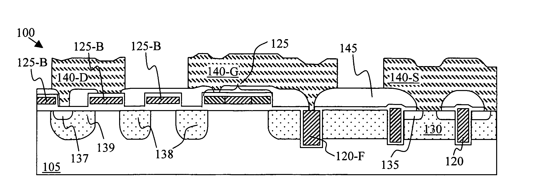
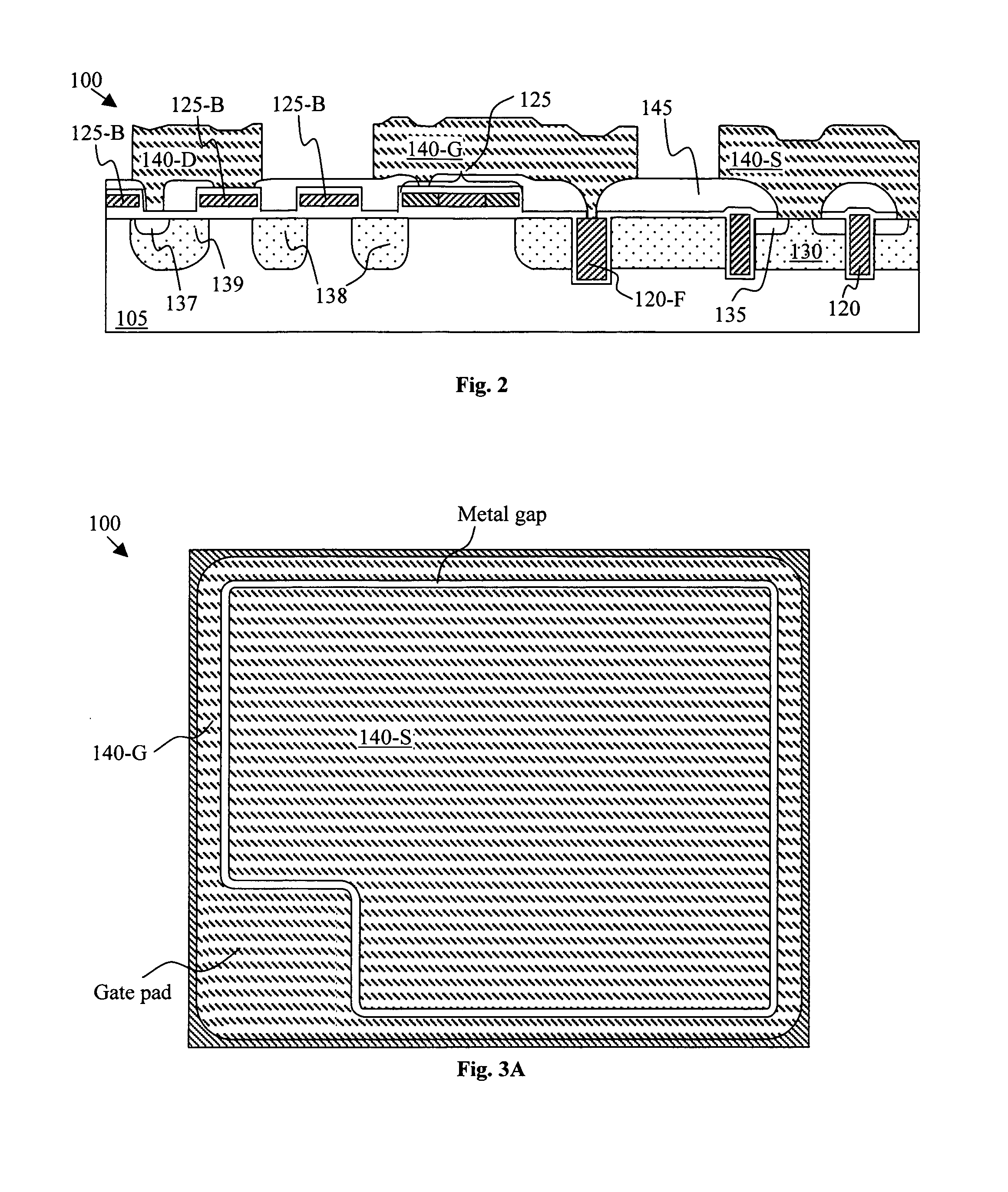
[0019]For simplicity only trench MOSFET device is illustrated. This invention applies to other types of trench power devices as well as planar power devices. Refer to FIG. 2 for a metal oxide semiconductor field effect transistor (MOSFET) device 100 of this invention. FIG. 2 shows a cross sectional view of the termination area and a portion of active area of the MOSFET device 100 that is supported on a semiconductor substrate 105 formed with trenched gates 120 surrounded by body regions 130 encompassing source region 135 therein. The MOSFET device 100 is covered by an oxide insulation layer 145 having gate contact opening for the gate metal 140-G to contact the trenched gate 120 through gate finger 120-F. The MOSFET device 100 is protected by ESD diodes 125 that typically formed on a polysilicon layer deposited on top of the substrate 100. In order to eliminate the requirement of a body block mask, there are polysilicon segments 125-B formed on top of the substrate 100 to function a...


PUM


Abstract

A semiconductor power device supported on a semiconductor substrate includes an electrostatic discharge (ESD) protection circuit disposed on a first portion of patterned ESD polysilicon layer on top of the semiconductor substrate. The semiconductor power device further includes a second portion of the patterned ESD polysilicon layer constituting a body implant ion block layer for blocking implanting body ions to enter into the semiconductor substrate below the body implant ion block layer. In an exemplary embodiment, the electrostatic discharge (ESD) polysilicon layer on top of the semiconductor substrate further covering a scribe line on an edge of the semiconductor device whereby a passivation layer is no longer required manufacturing the semiconductor device for reducing a mask required for patterning the passivation layer.

Description

BACKGROUND OF THE INVENTION[0001]1. Field of the Invention[0002]The invention relates generally to the configuration and manufacturing process of the semiconductor power devices. More particularly, this invention relates to an improved configuration for manufacturing an electrostatic discharge (ESD) protection circuit integrated with a semiconductor power device with reduced number of masks such that the semiconductor power device can be manufactured with simplified process, lower costs, improved production yield, and higher performance reliability.[0003]2. Description of the Prior Art[0004]Conventional layout for manufacturing semiconductor power devices with protection circuits against electrostatic discharges (ESD) still has a limitation. The conventional power MOSFET devices with ESD protection circuit generally have a layout and layer structures that requires application of seven masks in the typical manufacturing processes. These seven masks include a trench mask, an ESD mask,...

Claims


Application Information

Patent Timeline
Patent Type & Authority Applications(United States)
IPC IPC(8): H01L27/088H01L21/8234H01L29/06
CPCH01L27/0255H01L29/0619H01L29/0696H01L29/404H01L29/66734H01L29/7808H01L2924/0002H01L29/7811H01L29/7813H01L2924/00
Inventor BHALLA, ANUPWANG, XIAOBINWANG, WEISU, YING, DANIEL
Owner ALPHA & OMEGA SEMICON LTD
Why Eureka
Try Eureka