Diffractive optical device, and aligner comprising that device

a technology of diffractive optical and aligner, which is applied in the direction of photomechanical treatment, printers, instruments, etc., can solve the problems of limiting engendering other problems, and the efficiency of semiconductor exposure is much worse, so as to reduce the load on optical proximity correction, prevent a decrease in the quantity of light transmitting, and enhance the efficiency of semiconductor alignmen

Active Publication Date: 2009-07-02
DAI NIPPON PRINTING CO LTD
View PDF14 Cites 2 Cited by
  • Summary
  • Abstract
  • Description
  • Claims
  • Application Information

AI Technical Summary

Benefits of technology

[0019]In view of such problems as briefed above, the present invention has been made. That is, an object of the invention is to provide a pupil filter used with an illumination optical system for semiconductor aligners or the like, which works for preventing a decrease in the quantity of light transmitting through it, enhancing semiconductor alignment efficiency, cutting back on loads on optical proximity correction, and holding back fluctuations of the size of a pattern imaged on a wafer due to a mask pattern pitch, so making sure an optical image of stable yet high resolution.

Problems solved by technology

Only by use of such shorter wavelength and larger NA, there is still a limit to meeting this demand.
However, the changing of the illumination pupil filter from FIG. 10(a) to FIG. 10(b) is found to engender other problems.
One problem comes to arise when the pupil filter of FIG. 10(b) is achieved by an aperture (generally metal sheet machining); the quantity of light transmitting through the pupil filter of FIG. 10(b) diminishes or much time is taken for exposure, making the efficiency of semiconductor exposure much worse and, hence, semiconductor fabrication cost much.
This gives rise to another problem.
As the pattern pitch varies, however, it causes the contrast to change regularly or become erratic.
However, illumination light leaving the pupil filter is of high coherence; that is, there is a wider extent to which OPC must be applied, which imposes too much load to data processing, giving rise to a problem: correction by OPC is difficult, if not impossible.

Method used


Image

  • Diffractive optical device, and aligner comprising that device
  • Diffractive optical device, and aligner comprising that device
  • Diffractive optical device, and aligner comprising that device

Examples


examples

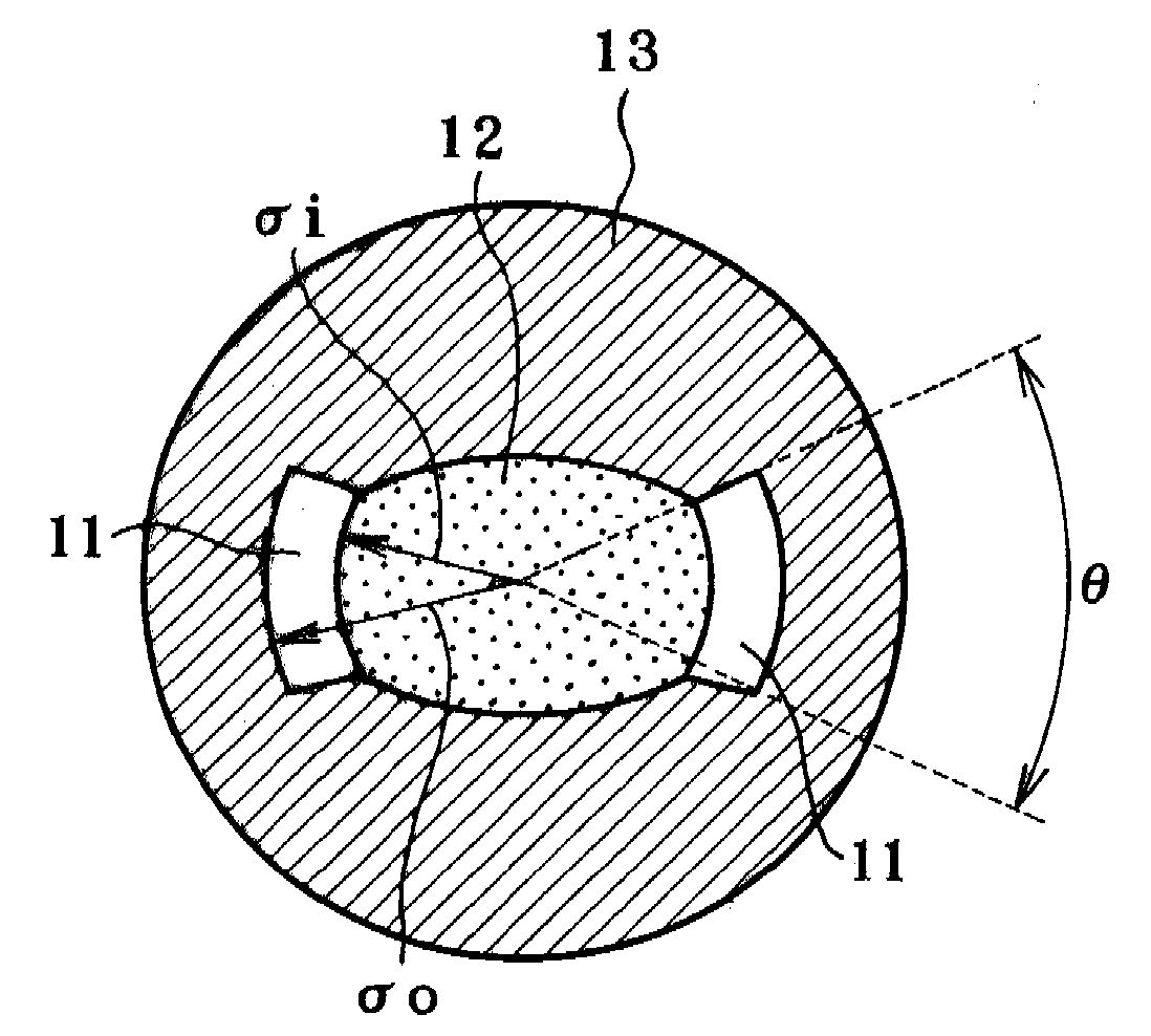
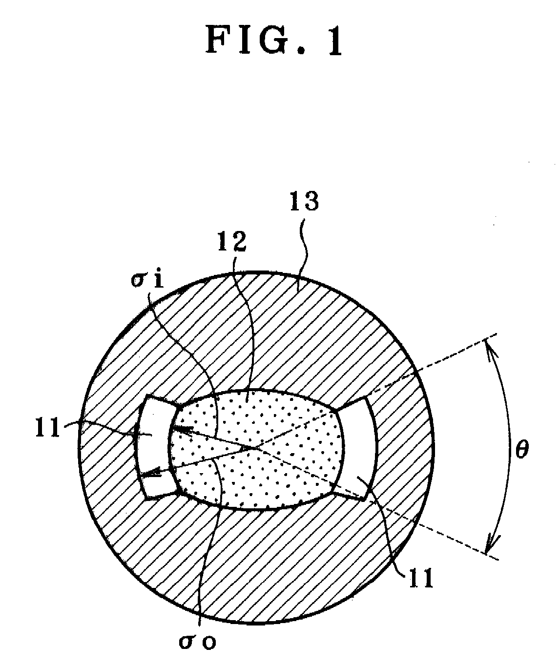
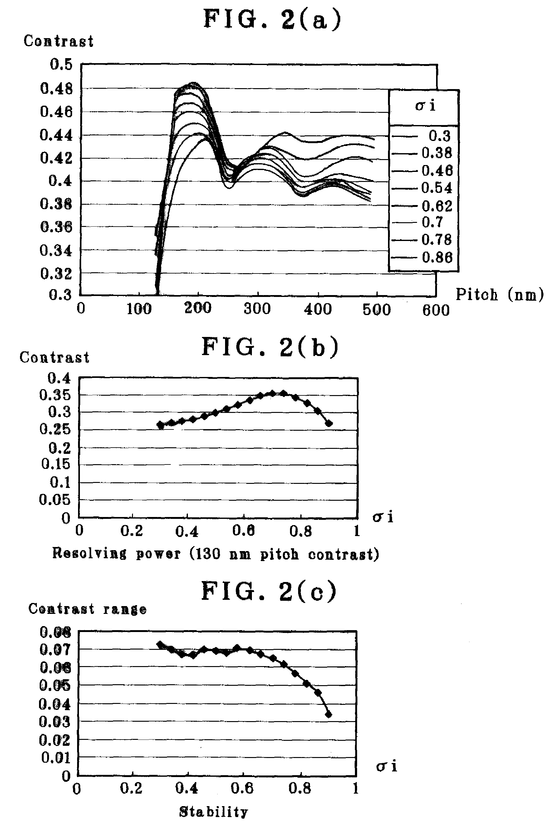
[0077]The invention is now explained in further details with reference to one specific example. This example is directed to a computer-generated hologram device having design specifications: the minimum pitch of the basic diffraction grating of 4,000 nm, the exit angle of 3.5° upon irradiation with illumination light, the 8 phase steps, and the transparent synthetic quartz substrate workpiece. Note here that the height specifications for each step were 193 nm, and the value of each part of the dipole pupil filter having two fan-form light transmissive areas formed by use of this diffractive optical device, too, was designed beforehand.

[0078]First, there was a photomask substrate readied up, which had a metal chromium film formed on one surface of an optically polished, transparent synthetic quartz substrate of 6 inches square and 6.35 mm thickness. After a positive type EB resist (ZEP7000 made by Nippon Zeon Co., Ltd.) was coated by rotational coating on the metal chromium film, dat...


PUM


Abstract

The invention relates to a pupil filter used for the illumination optical system of a semiconductor aligner or the like that can prevent a decrease in the quantity of light having transmitted through it, enhance the efficiency of semiconductor exposure, reduce loads of correction by the optical proximity effect and yield a stable yet high-resolution optical image without engendering size fluctuations of a pattern imaged on a wafer depending on a mask pattern pitch. Specifically, the invention provides a diffractive optical device for the formation of a pupil filter used for the illumination optical system of an aligner adapted to direct light emanating from a light source to a mask via an illumination optical system and project a pattern on the mask onto an alignment substrate and exposing it to light via a projection optical system. The pupil filter formed by the diffractive optical device is a dipole pupil comprising two light transmissive areas (11). The two light transmissive areas (11) are in a fan-form configuration symmetric at a given distance from the center of the pupil filter, between them there is an area (12) of low light transmittance, and outside the two light transmissive areas (11) and the area (12) of low light transmittance there is a light block area (13).

Description

TECHNICAL ART[0001]The present invention relates to a diffractive optical device for forming a pupil filter used for projection aligners utilized for the formation of semiconductor device patterns or the like, and an aligner comprising that diffractive optical device.BACKGROUND ART[0002]The step called generally photolithography is needed for the formation of circuit patterns for semiconductor devices. For this step, usually, there is a transfer process used, which transfers a photomask (often called the reticle, and hereinafter called simply the “mask” pattern onto the alignment substrate such as a semiconductor wafer. The alignment substrate is coated with a photosensitive photoresist, and a circuit pattern is transferred onto the photoresist depending on the pattern shape of the mask pattern. And at a projection aligner, the image of the circuit pattern written on the mask and to be transferred is projected onto the alignment substrate (wafer) and exposed to light by way of a pro...

Claims


Application Information

Patent Timeline
Patent Type & Authority Applications(United States)
IPC IPC(8): G03B27/72
CPCG03F7/70158G03F7/70108G02B5/18G02B5/1838
Inventor TOYAMA, NOBUHITOHORIGUCHI, RYUJI
Owner DAI NIPPON PRINTING CO LTD
Why Eureka
Try Eureka