Electronic component, semiconductor package, and electronic device

a technology of electronic components and semiconductors, applied in the field of electronic components, can solve the problems of reduced bonding strength, depletion of cu in the solder bump, and increasing the tendency of the alloy layer to fracture, and achieve excellent wettability with solder, high bonding strength, and high barrier characteristic

Inactive Publication Date: 2009-07-09
RENESAS ELECTRONICS CORP +1
View PDF5 Cites 33 Cited by
  • Summary
  • Abstract
  • Description
  • Claims
  • Application Information

AI Technical Summary

Benefits of technology

[0070]When solder bumps containing Sn are formed to electrically connect two or higher UBMs formed on the different electronic members, a CuNiSn alloy layer having an average Ni/Cu ratio of 2.3 or lower is formed between each pair of the UBMs and the solder bumps. As a result, generation of an Ni-rich CuNiSn alloy and a P-rich NiP or CuNiP layer can be suppressed while a high barrier charac

Problems solved by technology

In particular, when the solder inherently contains no Cu at all or when the amount of Cu in the solder is small, the alloy layer increasingly tends to fracture and hence the bonding strength decreases.
However, even in this case as well, the Cu in the solder bump is depleted when the electronic component is used in a high-temperature environment for an extended period.
As a result, the content of Cu in the interface between the UBM and the solder bump decreases, and an Ni-rich (Ni, Cu)3Sn4 or Ni3Sn4 intermetallic compound is gradually formed, resulting in an occurrence of phenomenon which ingenerates a fracture in the portion where such an intermetallic compound is formed and hence decreases the bonding strength.
Cracks may occur in the P-rich NiP layer, which is particularly hard but brittle among the above layers, and when a thermal stress impact, a drop impact, or other impacts are applied, the problem of the easier P-rich layer fracture occurs.
(c) Further, when electrode pads in an LSI are made of Al, a sufficient bonding strength between the solder bump and Al is not provided, and a UBM as an intermediate layer is therefore used.
In this case, when the barrier metal layer (UBM) used is made of a material having a poor barrier characteristic, such as Cu, and used in high-temperature conditions, the UBM is completely melted, resulting in the loss of the barrier characteristic.
Accordingly, there has been a problem that Al comes into direct contact with the solder bump, and the strength of the interface between the Al and the solder bump significantly decreases.
Therefore, there has been a problem that when the Cu film comes into contact with the solder b

Method used


Image

  • Electronic component, semiconductor package, and electronic device
  • Electronic component, semiconductor package, and electronic device
  • Electronic component, semiconductor package, and electronic device

Examples


first embodiment

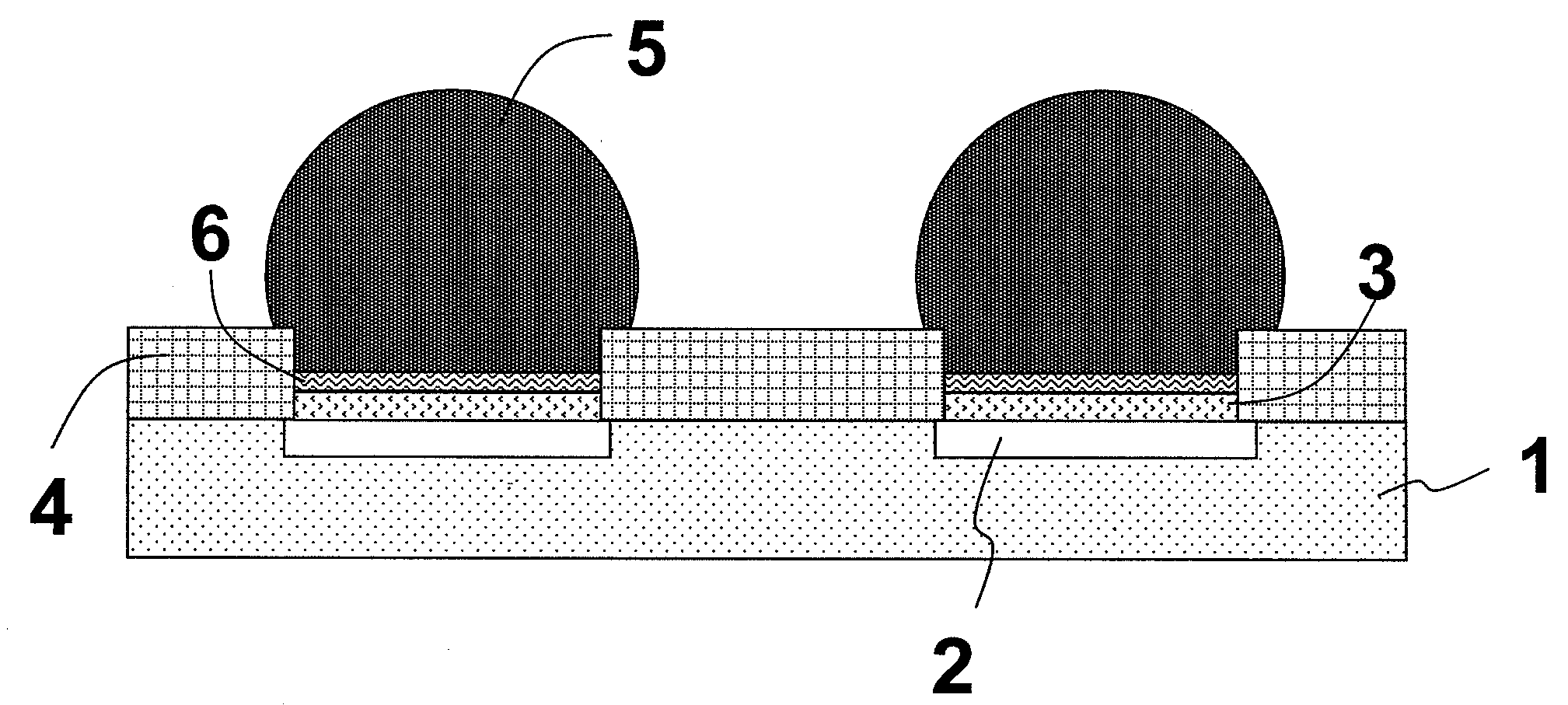
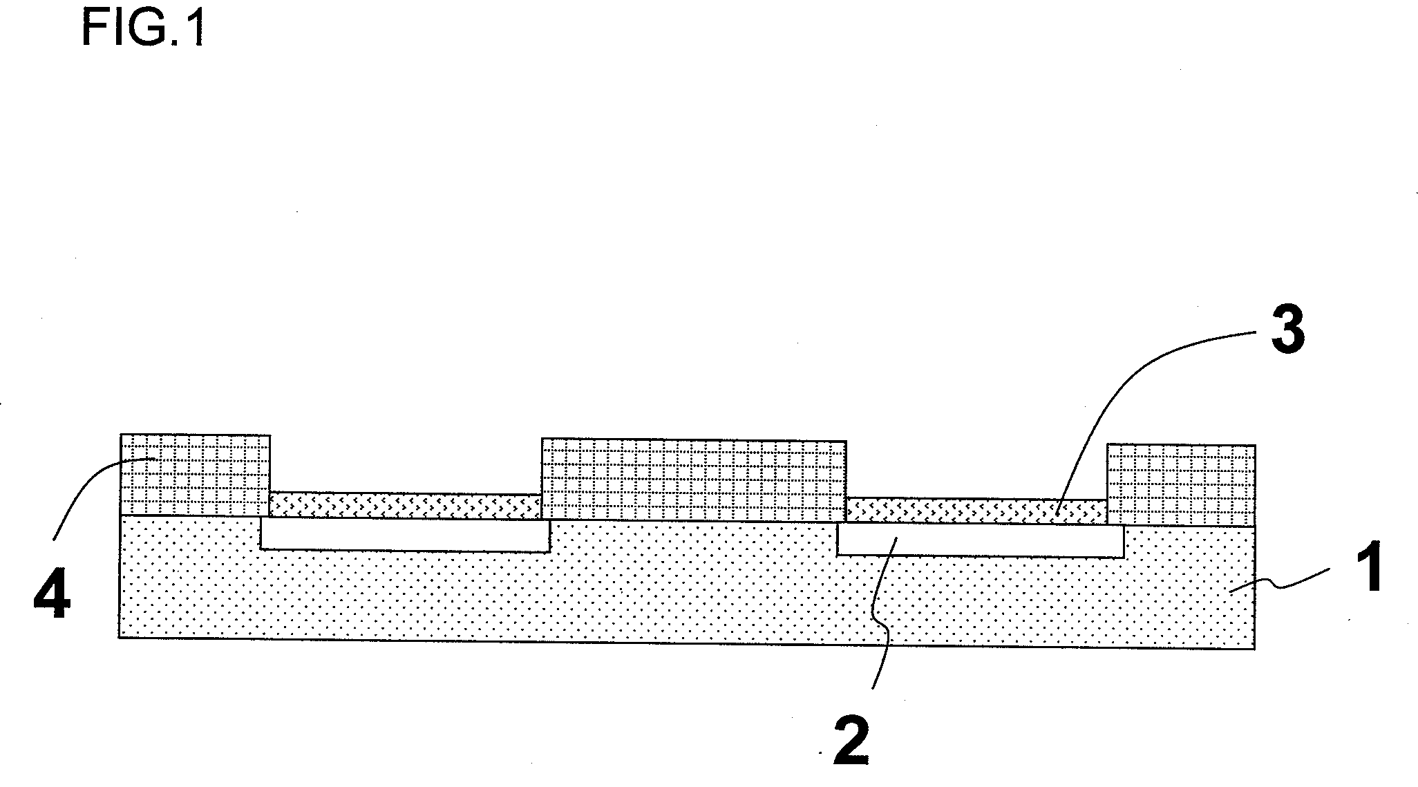
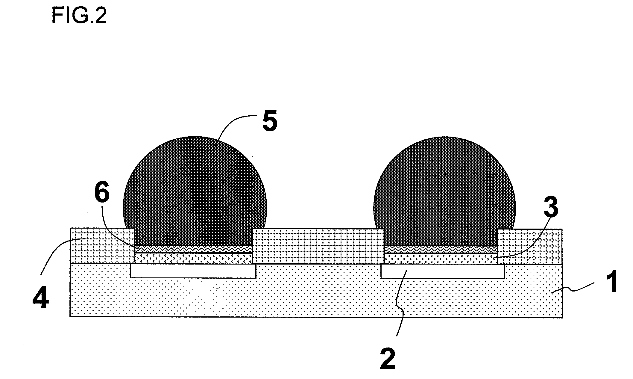
[0124]As shown in FIG. 1, in an example of an electronic component 1 according to the present invention, a UBM (barrier metal layer) 3 is formed on an electrode pad 2 made of, for example, Al, Cu, and Ag formed on a substrate or a semiconductor element. The electrode pad is electrically connected to a wiring in the substrate or the semiconductor element.

[0125]The UBM 3 has any of the following alloy layers formed at least on the side opposite the side in contact with the electrode pad: (1) a CuNi alloy layer containing 15 to 60 at % of Cu and 40 to 85 at % of Ni, (2) a CuNiP alloy layer containing 15 at % or higher of Cu, 40 at % or higher of Ni, and above Oat % and 25 at % or lower of P, or (3) a CuNiP alloy layer containing 44 to 60 at % of Cu, 29 to 40 at % of Ni, and 8 to 16 at % of P with the content of Ni (based on the number of atoms) being at least 2.5 times the content of P (based on the number of atoms).

[0126]That is, the CuNiP alloy layer (2) needs to contain 15 at % or h...

second embodiment

[0184]An electric component of the present invention may have, in addition to the structure described above, a structure having two or higher layers: an electrode pad 2 made of Al, Cu, Ag, or other elements and a CuNi alloy layer or CuNiP alloy layer 3 with an intermediate layer 9 therebetween, as shown in FIG. 10. In this case, the composition of the top barrier metal layer to be connected to a CuNiSn alloy layer needs to be a CuNi alloy or a CuNiP alloy.

[0185]Examples of the material of the intermediate layer 9 may include Ni, Cu, Pd, Pt, Fe, Co, Cr, and Ti, and NiP alloys, NiB alloys, and CoP alloys containing any of the above metals. The above alloys in the intermediate layer have the following composition:

[0186]NiP alloy: NiP alloy containing 2 to 25 at % of P[0187]NiB alloy: NiB alloy containing 1 to 10 at % of B[0188]CoP alloy: CoP alloy containing 2 to 25 at % of P

One reason of using the intermediate layer 9 is that the adhesion strength between a CuNi or CuNiP alloy layer a...

third embodiment

[0191]Electronic components that have been described in the present invention refer to components in general that form an electric circuit, such as those formed on a printed substrate, a flexible substrate, a ceramic substrate, a glass-ceramic substrate, and a semiconductor substrate, as well as chip capacitors and chip resistors.

[0192]A semiconductor package of the present invention has electronic members electrically connected via UBMs, solder bumps, and the like. Examples of the electronic member may include substrates (such as mother board substrates, interposer substrates, semiconductor packages, printed substrates, flexible substrates, ceramic substrates, glass-ceramic substrate, and semiconductor substrates) and semiconductor chips (semiconductor elements). Examples of connection between such electronic members may include substrate-to-substrate connection, semiconductor element-to-semiconductor element connection, and substrate-to-semiconductor element connection.

[0193]FIG. ...


PUM


Abstract

In a conventional UBM made of, for example, Cu, Ni, or NiP, there has been a problem that when an electronic component is held in high-temperature conditions for an extended period, the barrier characteristic of the UBM is lost and the bonding strength decreases due to formation of a brittle alloy layer at a bonding interface. The present invention improves the problem of decrease in long-term connection reliability of a solder connection portion after storage at high temperatures. An electronic component comprises the electronic component includes an electrode pad formed on a substrate or a semiconductor element and a barrier metal layer formed to cover the electrode pad and the barrier metal layer comprises a CuNi alloy layer on the side opposite the side in contact with the electrode pad, the CuNi alloy layer containing 15 to 60 at % of Cu and 40 to 85 at % of Ni.

Description

TECHNICAL FIELD[0001]The present invention relates to an electronic component, a semiconductor package, and an electronic device which comprise a barrier metal layer on an electrode pad.BACKGROUND ART[0002]In association with higher performance of electronic devices in recent years, there is an increasing need for higher density mounting in semiconductor packages. In an example of a method for providing such a high-density semiconductor package, solder bumps are formed on electrode pads on a surface of an LSI chip, and the LSI chip is joined with an interposer substrate or a mother board, such as a build-up substrate and a flexible substrate, or another LSI chip by using flip-chip connection.[0003]In general, when a solder bump made of, for example, SnPb, SnAg, SnCu, SnAgCu, SnZn, SnZnBi, and SnIn, is used in flip-chip connection, Sn, which the solder bump is primarily made of, diffuses into the electrode pad and wiring, made of Al or Cu, of an LSI chip during a reflow and bond proc...

Claims


Application Information

Patent Timeline
IPC IPC(8): H01L23/52
CPCH01L2224/05166H01L2224/05169H01L2224/05171H01L2224/05647H01L2224/05655H01L2224/1132H01L2224/11436H01L2224/1145H01L2224/11462H01L2224/1147H01L2224/115H01L2224/11502H01L2224/1152H01L2224/11849H01L2224/13022H01L2224/13111H01L2224/73204H01L2224/75702H01L2224/8121H01L2224/81447H01L2224/81455H01L2224/81815H01L2224/83104H01L2924/01002H01L2924/01005H01L2924/01007H01L2924/01011H01L2924/01013H01L2924/01015H01L2924/01022H01L2924/01027H01L2924/01028H01L2924/01029H01L2924/0103H01L2924/01033H01L2924/01046H01L2924/01047H01L2924/0105H01L2924/01074H01L2924/01078H01L2924/01079H01L2924/01082H01L2924/01327H01L2924/014H01L2924/09701H01L2924/15311H01L2924/19041H01L2924/19043H01L2924/3512H01L2924/3651H01L21/563H01L23/24H01L23/3128H01L23/49816H01L23/49866H01L24/03H01L24/05H01L24/11H01L24/13H01L24/16H01L24/75H01L24/81H01L2224/0345H01L2224/03462H01L2224/03464H01L2224/0362H01L2224/03828H01L2224/0401H01L2224/05073H01L2224/05082H01L2224/05083H01L2224/05084H01L2224/05118H01L2224/05147H01L2224/05155H01L2224/05157H01L2224/0516H01L2224/05164H01L2224/05571H01L2924/01006H01L2924/01024H01L2224/16225H01L2224/32225H01L2224/13006H05K3/244H05K3/3436H05K3/3463H01L2924/00014H01L2924/0002H01L2924/00H01L2224/05552H01L2924/15787H01L2924/181H01L2924/00012
Inventor SOGAWA, YOSHIMICHIYAMAZAKI, TAKAOTAKAHASHI, NOBUAKI
Owner RENESAS ELECTRONICS CORP
Why Eureka
Try Eureka