
Laminates, Thin-Film Sensors, Thin-Film Sensor Modules, and Methods for Producing the Thin-Film Sensors

a technology of thin film and sensor, applied in the direction of heat measurement, paper/cardboard containers, instruments, etc., can solve the problems of increasing costs, affecting the quality of thin film sensors, so as to improve sensitivity, increase the mean grain diameter of crystal grains, and increase the temperature coefficient of resistance

Inactive Publication Date: 2009-07-09
MITSUI MINING & SMELTING CO LTD
View PDF5 Cites 10 Cited by
  • Summary
  • Abstract
  • Description
  • Claims
  • Application Information

AI Technical Summary

Benefits of technology

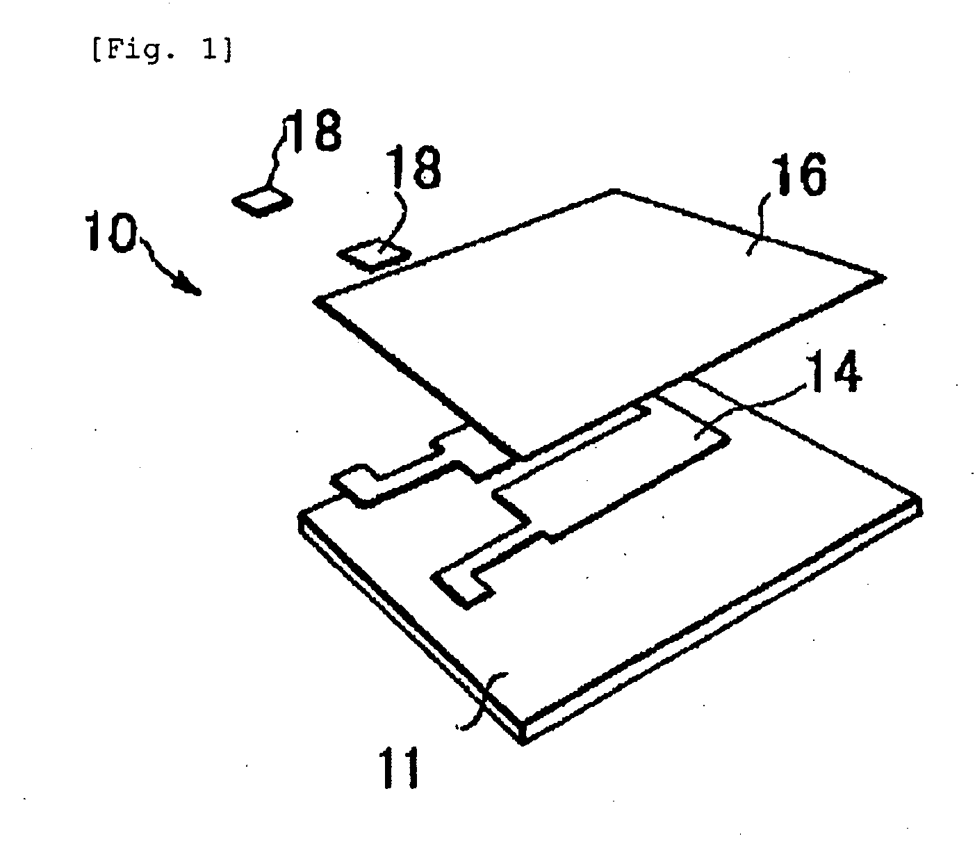
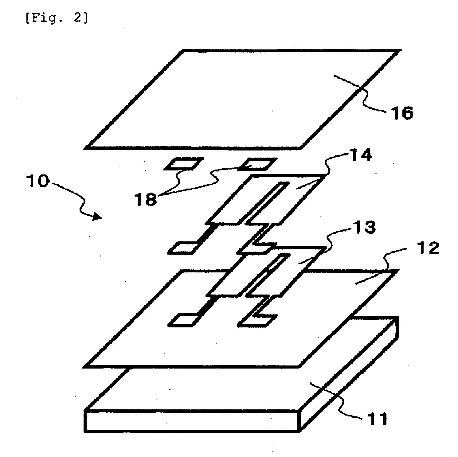
[0036]The present invention provides laminates suitable as a thin-film sensor, thin-film sensors comprising the laminate, thin-film sensor modules comprising the thin-film sensor, and methods for producing the thin-film sensors by controlling the orientation of crystals forming a temperature sensitive resistor.
[0037]One of the embodiments of the present invention provides laminates suitable as a thin-film sensor that is highly sensitive and in which a temperature-sensitive resistor is difficult to peel off, thin-film sensors comprising the laminate, thin-film sensor modules comprising the thin-film sensor, and methods for producing the thin-film sensors.
[0038]One of the embodiments of the present invention provides a thin-film sensor (thin-film sensor A) having an increased temperature coefficient of resistance of a temperature-sensitive resistor and an improved sensitivity, a thin-film sensor module comprising the thin-film sensor, and a method for producing the thin-film sensor by controlling the orientation of a crystal forming the temperature-sensitive resistor and the crystal structure to increase the mean grain diameter of crystal grains while suppressing the enormous enlargement of only a part of crystal grains and the increase of the surface roughness of a temperature-sensitive resistor.
[0039]One of the embodiments of the present invention provides a thin-film sensor (thin-film sensor B) that does not increase the surface roughness even by heat the treatment after film forming while obtaining the favorable electric properties, a thin-film sensor module comprising the thin-film sensor, and a method for producing the thin-film sensor

Problems solved by technology

Although higher sensitivity may be achieved by growing the crystal under severe heating conditions, such treatment entails a large amount of heat.
In addition, facilities capable of enduring such amount of heat are necessary, which adds costs.
Further, heat treatment increases the surface roughness of a thin-film sensor and causes low production stability.
Furthermore, satisfactory electrical properties (temperature coefficient of resistance, TCR, and the like) have not been obtained only by heat treatment.
However, the adhesion between the platinum thin-film and the substrate is still insufficient.

Method used


Image

  • Laminates, Thin-Film Sensors, Thin-Film Sensor Modules, and Methods for Producing the Thin-Film Sensors
  • Laminates, Thin-Film Sensors, Thin-Film Sensor Modules, and Methods for Producing the Thin-Film Sensors
  • Laminates, Thin-Film Sensors, Thin-Film Sensor Modules, and Methods for Producing the Thin-Film Sensors

Examples


example 1

[0175]A SiO2 layer was formed on an aluminum substrate by the similar operation to that of Example 1. Thereafter, a titanium layer having a film thickness of 30 nm was formed in the same manner as Comparative Example 1 except that the conditions of forming a titanium layer were changed to the following conditions.

[0176]Apparatus: Magnetron sputtering apparatus

[0177]Ultimate vacuum: Less than 2.0×10⁻⁵ Pa

[0178]Film-forming pressure: 0.03 Pa

[0179]Gas flow rate: 20 SCCM [Ar:O2=10:0 (volume ratio at standard state)]

[0180]Film-forming electric power: 50 W (DC)

[0181]Film-forming temperature: 400° C.

[0182]Next, a temperature-sensitive resistor having a film thickness of 400 nm was formed on the titanium layer thus formed by performing sputtering using platinum (purity: 99.9%) as a target under the following conditions.

[0183]Apparatus: Magnetron sputtering apparatus

[0184]Ultimate vacuum: Less than 2.0×10⁻⁵ Pa

[0185]Film-forming pressure: 0.03 Pa

[0186]Gas flow rate: 20 SCCM [Ar:O2=10:0 (volume...

example 2

[0192]A thin-film sensor 2 (a temperature sensor 2) was obtained by heat treating the laminate 1 at 1,000° C. for 4 hours under an atmospheric atmosphere. The thin-film sensor 2 was tested for temperature coefficient of resistance (TCR), crystal grain diameters, orientation properties and adhesion as described below. The results are shown in Table 1. In addition, the measurement of the pole figure for (111) planes was made. The result is shown in FIG. 7.

example 3

[0193]A thin-film sensor 3 (a temperature sensor 3) was obtained by heat treating the laminate 1 at 900° C. for 4 hours under an atmospheric atmosphere (oxygen partial pressure: 20%). The thin-film sensor 3 was tested for temperature coefficient of resistance (TCR), crystal grain diameters, orientation properties and adhesion as described below. The results are shown in Table 1.


PUM

PropertyMeasurementUnit
Temperatureaaaaaaaaaa
Fractionaaaaaaaaaa
Fractionaaaaaaaaaa

Abstract

A laminate includes an insulating substrate, and a temperature-sensitive resistor made of crystals of a metal based on a platinum group element and laminated on the insulating substrate; and has a percentage of (111) planes of crystals oriented at 10° or less from the normal direction (ND direction) in a layer of the temperature-sensitive resistor being 90% or more. By controlling the orientation of crystals forming the temperature-sensitive resistor, laminates suitable as a thin-film sensor, thin-film sensors including the laminate, thin-film sensor modules including the thin-film sensor, and methods for producing the thin-film sensors are provided.

Description

TECHNICAL FIELD[0001]The present invention relates to laminates, thin-film sensors, thin-film sensor modules and methods for producing the thin-film sensors.BACKGROUND ART[0002]Thin-film sensor modules are used in temperature sensors and the like to enable them to perform their function of measuring temperature of objects or fluids. Thin-film sensor modules having temperature-sensitive resistors are widely used. They convert changes in amount of heat into electric signals and detect temperatures. From the viewpoint of sensitivity in particular, thin-film sensor modules that have platinum elements with a large absolute value of temperature coefficient of resistance are common. However, enhanced resistivity is still needed.[0003]As generally known in the art, the temperature coefficients of resistance of resistors change depending on the existence form of crystals forming the resistors (Non-patent Document 1). For example, Patent Document 1 and Non-patent Document 2 disclose technique...

Claims


Application Information

Patent Timeline
IPC IPC(8): H01C7/00C23C14/34B32B37/00
CPCG01K7/183Y10T156/10H01C17/075H01C7/006
Inventor WADA, MITSUHIROIKEDA, MAKOTOTOMONARI, KENJIINOUE, SHINICHISEKIMORI, HIDESHI
Owner MITSUI MINING & SMELTING CO LTD
Learn More