Hybrid orientation substrate compatible deep trench capacitor embedded dram

a capacitor and hybrid orientation technology, applied in the field of semiconductor devices, can solve problems such as inability to alleviate problems and compromise the integrity of the spacer

Inactive Publication Date: 2009-07-09
GLOBALFOUNDRIES INC
View PDF19 Cites 25 Cited by
  • Summary
  • Abstract
  • Description
  • Claims
  • Application Information

AI Technical Summary

Benefits of technology

[0007]In the present invention, method of limiting the lateral extent of a trench capacitor by a dielectric spacer in a hybrid orientations substrate is provided. The dielectric spacer separates a top semiconductor portion from an epitaxially regrown portion, which have different crystallographic orientations. A deep trench is formed in two stages. In the first stage, the deep trench is formed as a substantially straight trench within the epitaxially regrown portion such that part of the epitaxially regrown portion remains overlying the dielectric spacer. In the second stage, the substantially straight trench is laterally expanded to form a bottle shaped trench and to provide increased capacitance. The lateral expansion of the deep trench is self-limited by the dielectric spacer above the interface between the handle substrate and the buried insulator layer During subsequent formation of a doped buried plate, the dielectric spacer blocks diffusion of dopants into the top semiconductor portion, providing a compact bottle shaped trench capacitor having high capacitance without introducing dopants into the top semiconductor portion.

Problems solved by technology

This problem is not alleviated even on a hybrid orientation substrate.
A spacer can be formed on the trench sidewall of the top semiconductor layer to prevent diffusion of dopants (see U.S. Pat. No. 6,566,177 to Radens et al., for example), but the spacer is susceptible to erosion during deep trench etch and consequently the integrity of the spacer is compromised.

Method used


Image

  • Hybrid orientation substrate compatible deep trench capacitor embedded dram
  • Hybrid orientation substrate compatible deep trench capacitor embedded dram
  • Hybrid orientation substrate compatible deep trench capacitor embedded dram

Examples


Embodiment Construction

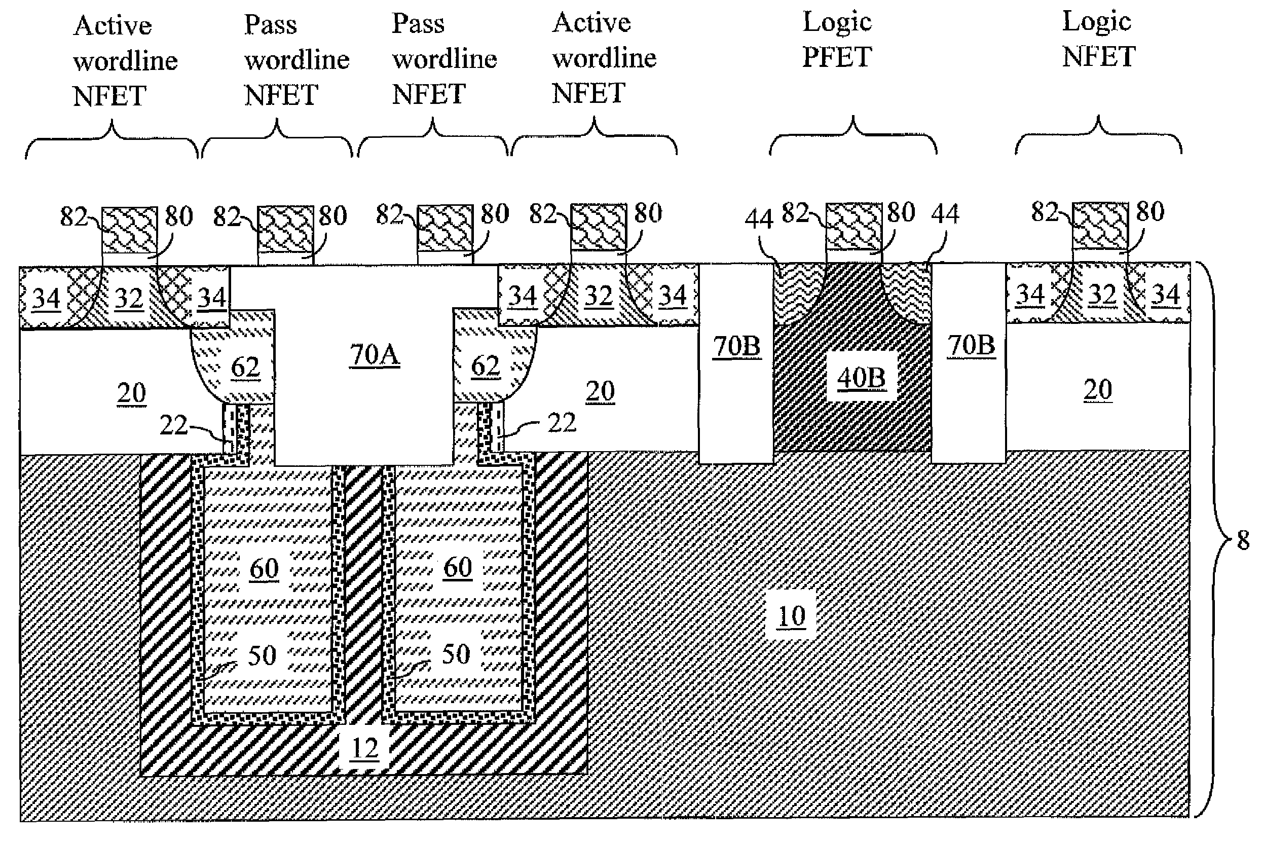
[0028]As stated above, the present invention relates to a dynamic random access memory (DRAM) or an embedded dynamic random access memory (eDRAM) employing a deep trench capacitor and formed in a hybrid orientation substrate, and methods of manufacturing the same, which are now described in detail with accompanying figures. It is noted that like and corresponding elements mentioned herein and illustrated in the drawings are referred to by like reference numerals.

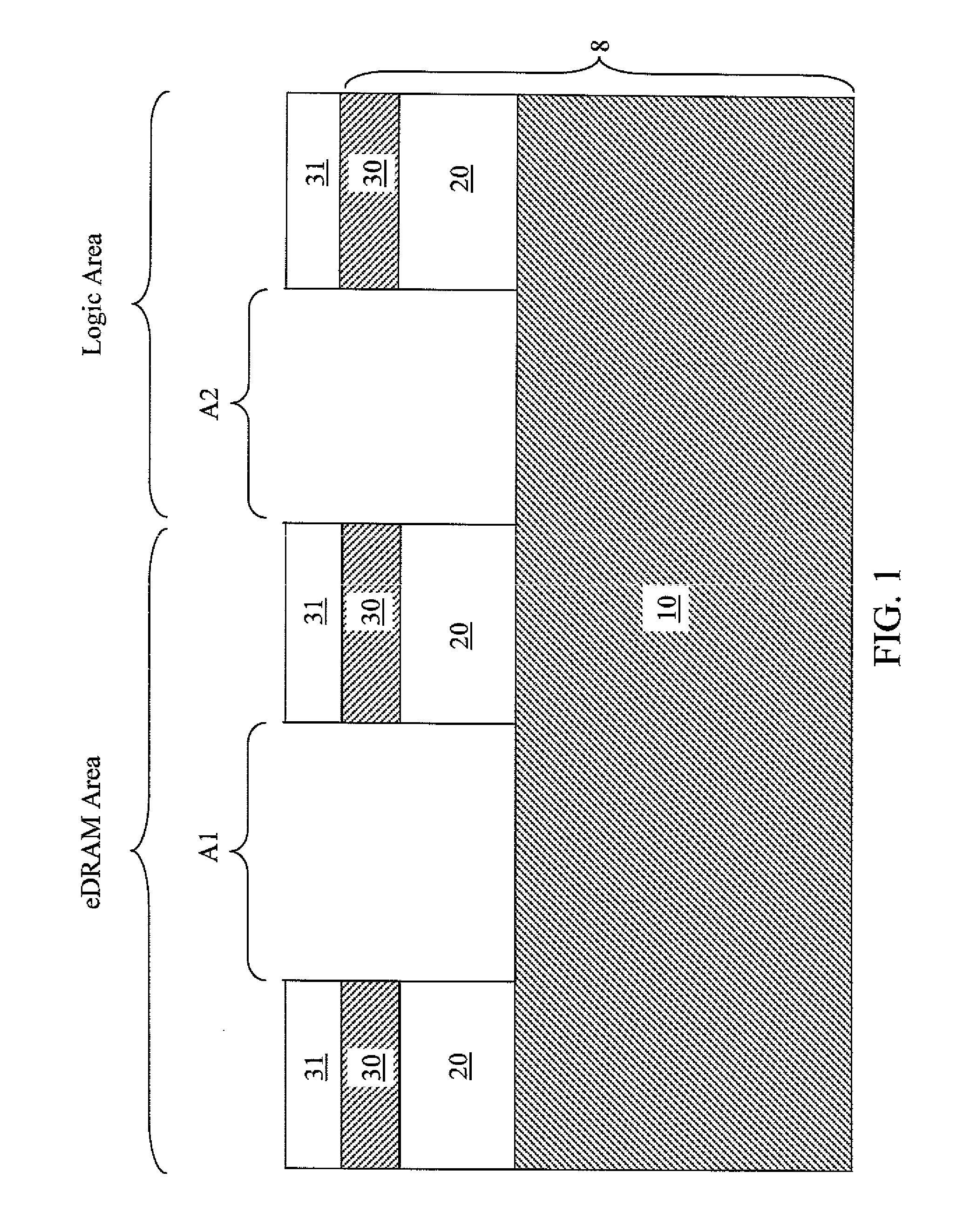
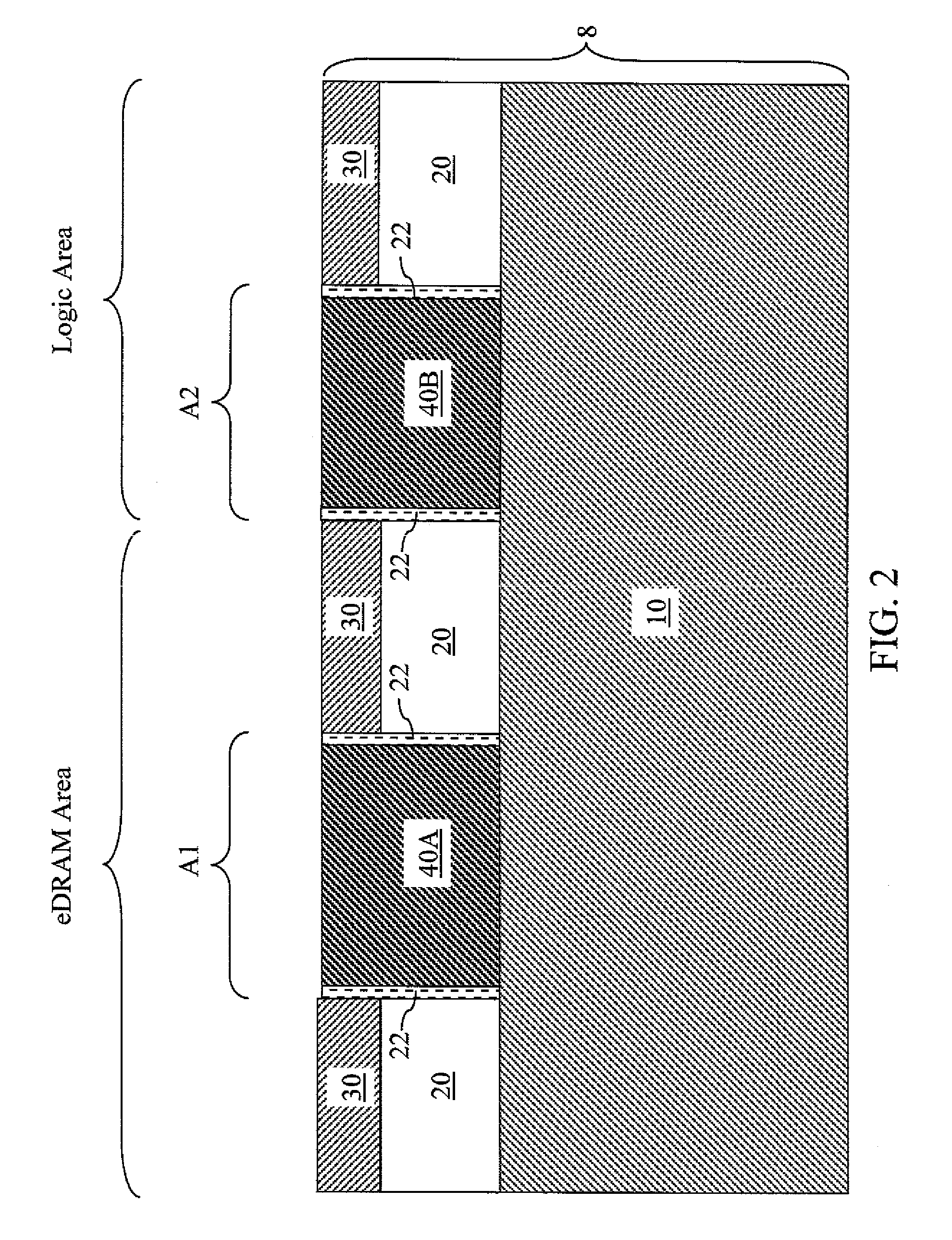
[0029]Referring to FIG. 1, an exemplary semiconductor structure according to the present invention comprises a semiconductor substrate 8. The semiconductor substrate 8 contains a handle substrate 10, a buried insulator layer 20, and top semiconductor portions 30. Each of the handle substrate 10 and the top semiconductor portions 30 comprises a semiconductor material, which may be selected from, but is not limited to, silicon, germanium, a silicon-germanium alloy, a silicon carbon alloy, a silicon-germanium-carbon alloy, gall...


PUM


Abstract

Method of limiting the lateral extent of a trench capacitor by a dielectric spacer in a hybrid orientations substrate is provided. The dielectric spacer separates a top semiconductor portion from an epitaxially regrown portion, which have different crystallographic orientations. The deep trench is formed as a substantially straight trench within the epitaxially regrown portion such that part of the epitaxially regrown portion remains overlying the dielectric spacer. The substantially straight trench is then laterally expanded to form a bottle shaped trench and to provide increased capacitance. The lateral expansion of the deep trench is self-limited by the dielectric spacer above the interface between the handle substrate and the buried insulator layer. During subsequent formation of a doped buried plate, the dielectric spacer blocks diffusion of dopants into the top semiconductor portion, providing a compact bottle shaped trench capacitor having high capacitance without introducing dopants into the top semiconductor portion.

Description

FIELD OF THE INVENTION [0001]The present invention relates to semiconductor structures, and particularly to an embedded dynamic random access memory (eDRAM) employing a deep trench capacitor and formed in a hybrid orientation substrate, and methods of manufacturing the same.BACKGROUND OF THE INVENTION [0002]Deep trenches, typically having a depth exceeding 1 micrometer, or 1 micron, in contrast to shallow trenches having a depth less than 1 micron, are employed in the semiconductor industry to provide a variety of useful devices including a deep trench capacitor. The deep trenches may be utilized in a stand-alone semiconductor circuit such as a dynamic random access memory (DRAM) circuit to provide deep trench capacitors, or may be utilized as an embedded circuit component of a semiconductor chip that also includes other semiconductor circuits such as a processor core or other logic circuits. Particularly, embedded capacitors employing a deep trench are employed to enable an embedde...

Claims


Application Information

Patent Timeline
Patent Type & Authority Applications(United States)
IPC IPC(8): H01L21/20
CPCH01L21/823807H01L21/84H01L27/0629H01L27/10829H01L29/66181H01L27/10894H01L27/10897H01L27/1203H01L27/1087H10B12/37H10B12/0387H10B12/50H10B12/09
Inventor CHENG, KANGGUODIVAKARUNI, RAMACHANDRA
Owner GLOBALFOUNDRIES INC
Why Eureka
Try Eureka