Plasma processing apparatus, plasma processing method and photoelectric conversion element

a plasma processing and plasma technology, applied in the direction of sustainable manufacturing/processing, final product manufacturing, coatings, etc., can solve the problems of complicated mechanism, unavoidable complex mechanical structure of intermediate chambers, and stoppage of whole production lines, so as to reduce plasma processing speed and reduce time-averaged value of applied power , the effect of easy control of throughpu

Inactive Publication Date: 2009-07-23
SHARP KK
View PDF5 Cites 35 Cited by
  • Summary
  • Abstract
  • Description
  • Claims
  • Application Information

AI Technical Summary

Benefits of technology

[0055]According to the invention, when at least two plasma processing steps are performed in the same plasma reaction chamber, one of the steps can perform the plasma processing using the CW AC power, and the other step can perform the plasma processing using the pulse-modulated AC power. Thereby, the plasma processing can be performed in various manners even in the step of which plasma processing conditions are limited due to the apparatus configuration.
[0056]Also, according to the invention, when at least two plasma processing steps of which discharge start voltages are different from each other are performed in the same plasma reaction chamber, respectively, the first plasma processing step performed with the low discharge start voltage uses the CW AC power as the plasma processing power, i.e., the power for the plasma processing, and the second plasma processing step performed with the high discharge start voltage uses the pulse-modulated AC power as the plasma processing power. Thereby, even in the second plasma processing step performed with the high discharge start voltage, a high voltage can be applied between the cathode and anode, and the time-averaged value of the applied power can be reduced. According to the invention, therefore, the uniform plasma can be generated and kept between the electrodes, and the plasma processing speed can be reduced so that the throughput can be controlled easily.
[0057]Further, the invention can achieve the following ef

Problems solved by technology

However, for manufacturing such silicon-base thin film photoelectric conversion elements, it has been required to reduce further a cost of a manufacturing apparatus such as a CVD apparatus that is a primary apparatus for device production, and this is an issue to be addressed for spreading the photoelectric conversion elements on a large scale.
This results in a problem that the whole production line is stopped even when it is necessary to maintain only one reaction chamber forming

Method used


Image

  • Plasma processing apparatus, plasma processing method and photoelectric conversion element
  • Plasma processing apparatus, plasma processing method and photoelectric conversion element
  • Plasma processing apparatus, plasma processing method and photoelectric conversion element

Examples


first embodiment

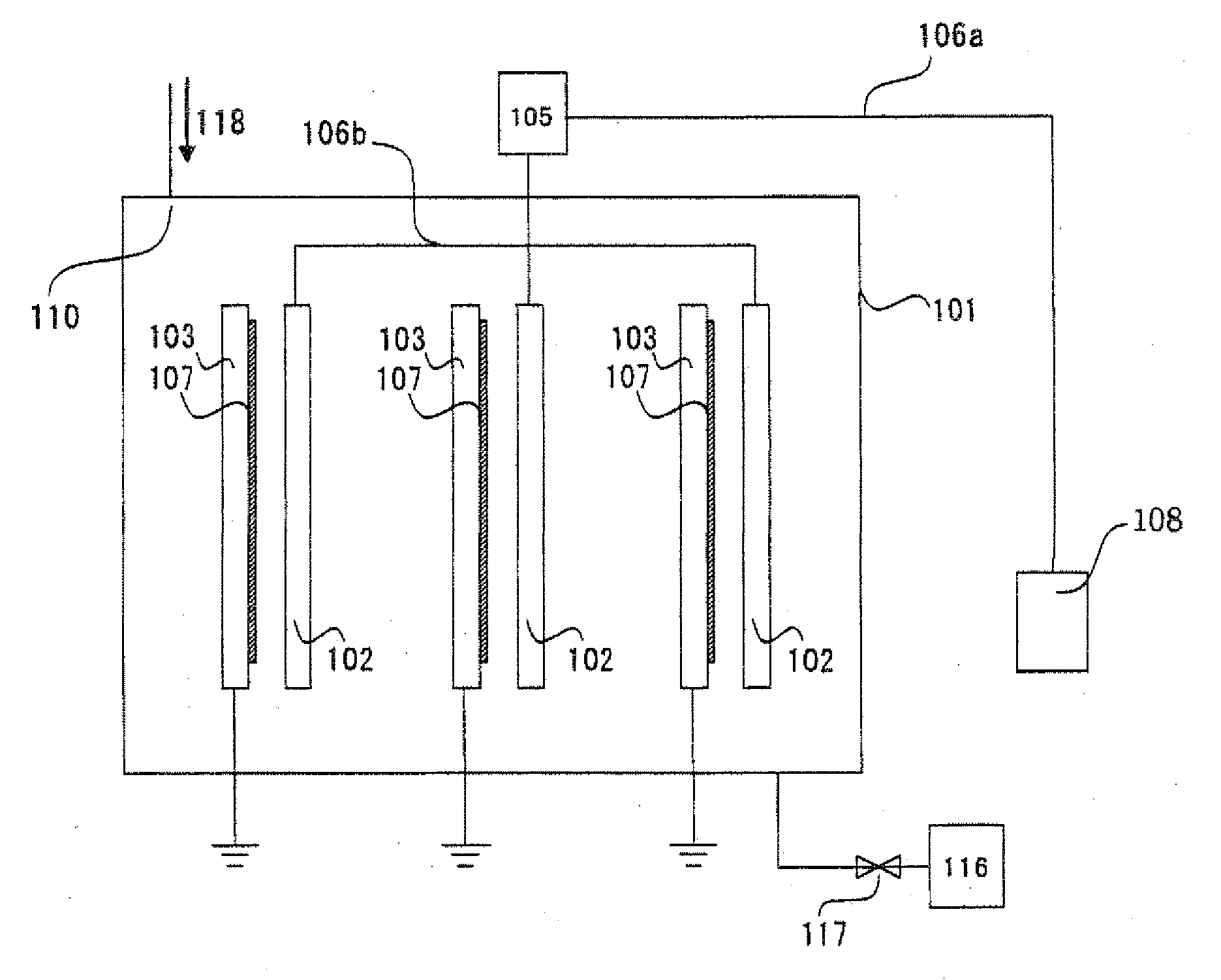
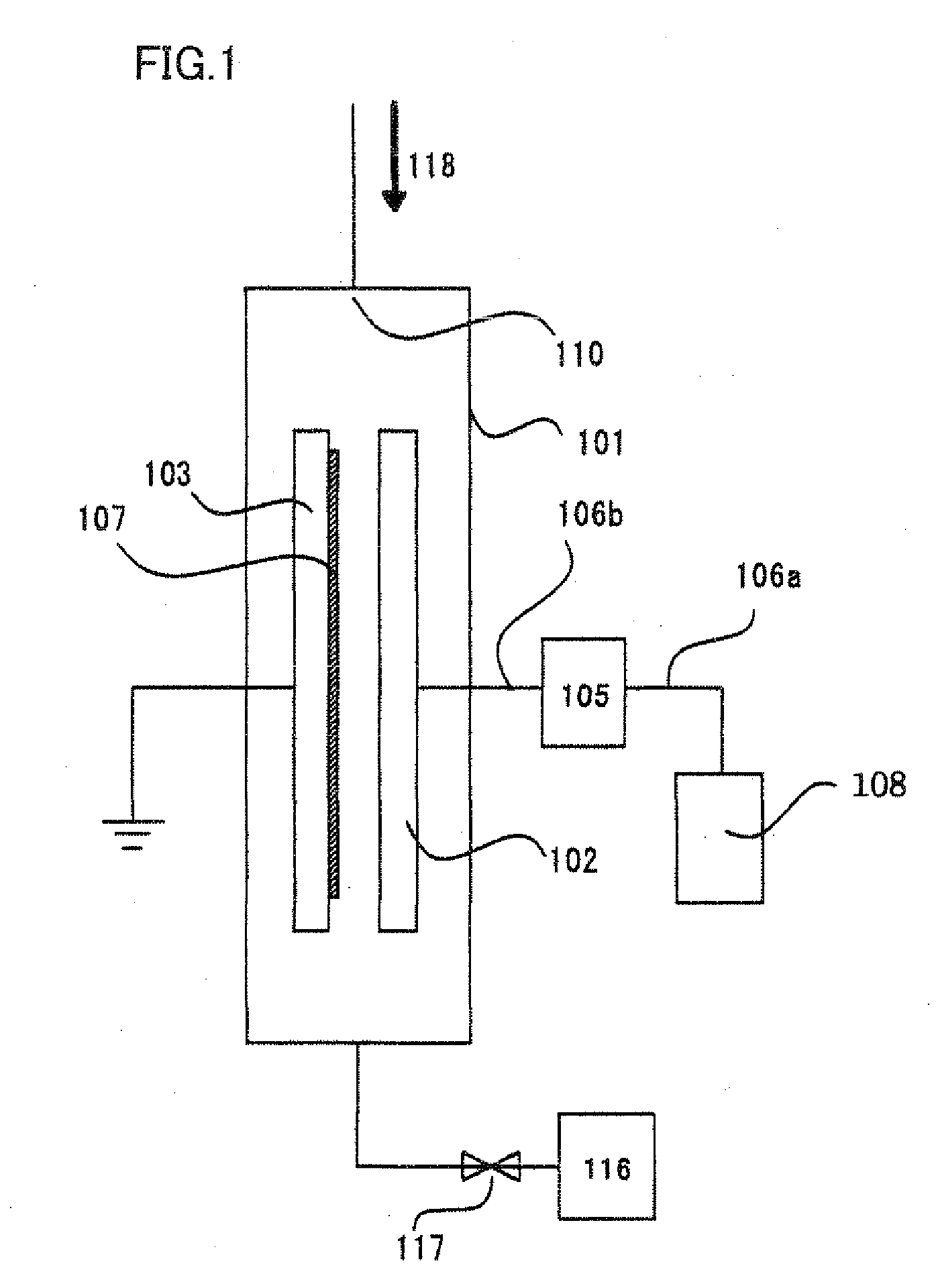
[0084]A plasma processing apparatus and method according to this embodiment are configured to deposit semiconductor layers of a thin film amorphous silicon photoelectric conversion element having a pin structure on work 107 by the plasma CVD method in the same plasma reaction chamber 101.

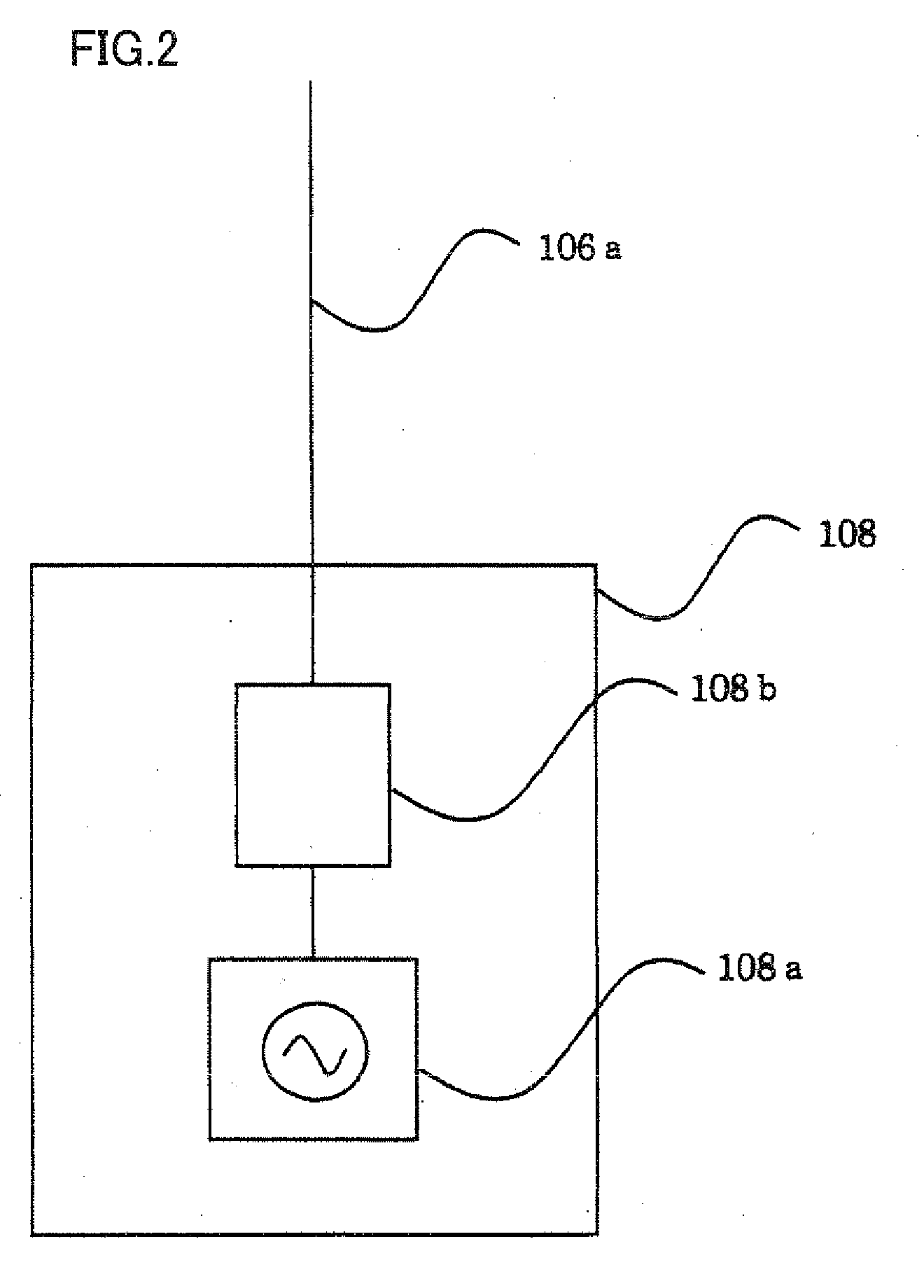
[0085]The p-type amorphous silicon layer and the i-type amorphous silicon layer are deposited using a pulse-modulated AC power as a power supply for the plasma processing (a second plasma processing step), and the n-type amorphous silicon layer is deposited using a CW AC power as a power supply for the plasma processing (a first plasma processing step).

[0086]The p-type amorphous silicon layer can be deposited under the following deposition conditions. The pressure in plasma reaction chamber 101 during the deposition is desirably in a range from 200 Pa to 3000 Pa, and is 400 Pa in this embodiment. A base temperature of a substrate 201 is desirably 250° C. or lower, and is 180° C. in this embodiment. ...

second embodiment

[0099]A plasma processing apparatus and method according to the embodiment execute a plasma CVD step (i.e., a step including a first plasma processing step) of depositing a thin film on work 107 by a plasma CVD method, and a plasma etching step (a second plasma processing step) of etching another work 107 in the same plasma reaction chamber 101.

[0100]The plasma CVD step is merely required to have at least one first plasma processing step using a CW AC power, and may further include a plasma CVD step using a pulse-modulated AC power. The plasma CVD step may be a step of depositing a film of a single layer, may also be a step of depositing a layer of multiple layers. In this embodiment, a film of multiple layers is deposited by the plasma CVD step.

[0101]Conversely, the plasma etching step performs the plasma etching using a pulse-modulated AC power, and a discharge start voltage thereof is higher than that in the first plasma processing step.

[0102]This embodiment will now be described...

third embodiment

[0108]In a plasma processing apparatus and method according to this embodiment, at least two plasma CVD steps of which discharge start voltages are different from each other are executed in the same plasma reaction chamber 101. As an example thereof description will now be given on a plasma processing apparatus and method that deposit a semiconductor layer of a silicon-base thin film photoelectric conversion element.

[0109]It is noted that the effect of the invention that is achieved by the following embodiment can likewise be achieved by such a semiconductor layer forming step of a silicon-base thin film photoelectric conversion element that includes a step of forming an i-type amorphous silicon-base photoelectric conversion layer by a pulse-modulated AC power and a step of forming an i-type crystalline silicon-base photoelectric conversion layer by a CW AC power.

[0110]The plasma processing apparatus implementing the embodiment is similar to that shown in FIG. 1.

[0111]FIG. 4 is a sc...


PUM

PropertyMeasurementUnit
Pressureaaaaaaaaaa
Speedaaaaaaaaaa
Electric potential / voltageaaaaaaaaaa

Abstract

In the case of performing at least two plasma processing steps in a common plasma reaction chamber, a CW AC power or a pulse-modulated AC power is appropriately selected as a power for plasma processing in each step. Thereby, even in a step where plasma processing conditions are limited due to apparatus configurations, the plasma processing can be performed in more various manners. Further, uniform plasma can be generated between electrodes and a quantity of a power to be supplied between the electrodes can be reduced, by using the pulse-modulated AC power. Thereby, a plasma processing speed can be reduced so that throughput control is facilitated.

Description

TECHNICAL FIELD[0001]The invention relates to a plasma processing apparatus, plasma processing method and photoelectric conversion element. Particularly, the invention relates to a plasma processing apparatus provided with a supply unit that supplies a CW (Continuous Waveform) AC power and a pulse-modulated AC power to a common plasma reaction chamber, a plasma processing method performing at least two plasma processing steps using the plasma processing apparatus, and a photoelectric conversion element manufactured by the above method. More specifically, the invention relates to a plasma processing apparatus and method that form at least an i-type amorphous silicon-base photoelectric conversion layer and an i-type crystalline silicon-base photoelectric conversion layer by a plasma CVD (Chemical Vapor Deposition) method, and also relates to a silicon-base thin film photoelectric conversion element.BACKGROUND ART[0002]In recent years, silicon-base thin film photoelectric conversion el...

Claims


Application Information

Patent Timeline
IPC IPC(8): H01L31/00C23C16/00H01L21/306
CPCC23C16/24C23C16/509H01J37/32091Y02E10/548H01L31/076H01L31/204H01J37/32137Y02P70/50
Inventor SANNOMIYA, HITOSHINAKANO, TAKANORI
Owner SHARP KK
Why Eureka
Try Eureka