Semiconductor device and fabrication method of the semiconductor device

a semiconductor device and semiconductor technology, applied in the direction of semiconductor devices, electrical devices, transistors, etc., can solve the problems of large current collapse, large amount of leakage current, and extreme deformation of the high frequency characteristics of the semiconductor device, so as to achieve high resistivity, improve the high frequency characteristics, and highly efficient semiconductor

Inactive Publication Date: 2009-07-30
KK TOSHIBA
View PDF2 Cites 30 Cited by
  • Summary
  • Abstract
  • Description
  • Claims
  • Application Information

AI Technical Summary

Benefits of technology

[0026]According to the present invention, piezo charge can be inactivated, high frequency characteristics can be improved by obtaining a high resistivity semiconductor layer, and a highly efficient semiconductor device and a fabrication method of the semiconductor device can be provided, by impurity doping the transition metal atom in the gallium nitride (GaN) layer which sandwiches the upper and lower sides of the AlGaN layer or the AlN layer.
[0027]Moreover, according to the present invention, a crystal defect of the GaN layer is reduced, an amount of leakage current and an amount of current collapse can be reduced, and a semiconductor device of stable high frequency performance and a fabrication method of the semiconductor device can be provided.

Problems solved by technology

It is known that FETs (Field Effect Transistors) using a GaN (gallium nitride) related semiconductor have a large amount of current collapse and have a large amount of leakage current.
Therefore, there was a problem that the amount of electric charges induced in the GaN layer degrades the high frequency performance of the semiconductor device extremely.
Therefore, there is a problem that the amount of electric charges induced in the GaN layer 120 degrades the high frequency characteristics of the semiconductor device extremely.
Therefore, there is a problem that the amount of electric charges induced in the GaN layer 200 degrades the high frequency characteristics of a semiconductor device extremely.

Method used


Image

  • Semiconductor device and fabrication method of the semiconductor device
  • Semiconductor device and fabrication method of the semiconductor device
  • Semiconductor device and fabrication method of the semiconductor device

Examples


first embodiment

(Device Structure)

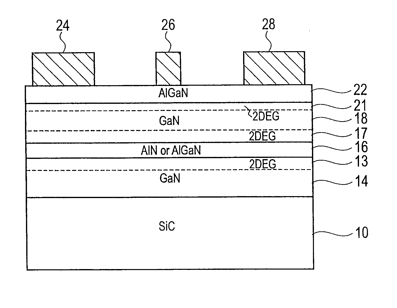
[0034]As shown in FIG. 2, a semiconductor device according to a first embodiment of the present invention includes: a substrate 10; a nitride based compound semiconductor layer 14 which is placed on the substrate 10 and is doped with a first transition metal atom; an aluminum gallium nitride layer (AlxGa1-xN) (where 0.116 placed on the nitride based compound semiconductor layer 14 doped with the first transition metal atom; a nitride based compound semiconductor layer 18 which is placed on the aluminum gallium nitride layer (AlxGa1-xN) (where 0.116, and is doped with a second transition metal atom; an aluminum gallium nitride layer (AlyGa1-yN) (where 0.122 placed on the nitride based compound semiconductor layer 18 doped with the second transition metal atom; and a gate electrode 26, a source electrode 24, and a drain electrode 28 which are placed on the aluminum gallium nitride layer (AlyGa1-yN) (where 0.122.

[0035]A two-dimensional electron gas layer 13 is formed ...

second embodiment

(Device Structure)

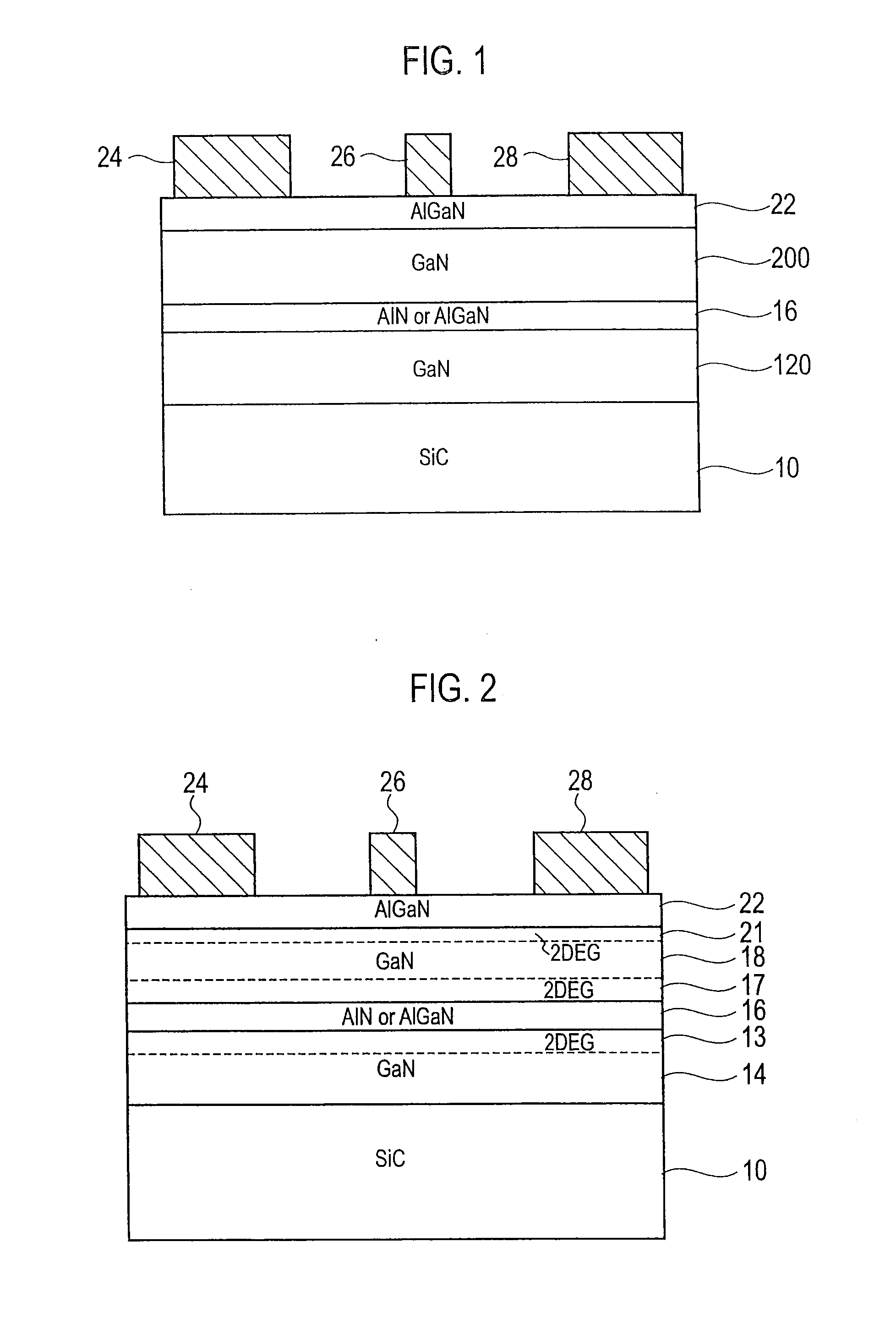
[0049]As shown in FIG. 3, a semiconductor device according to a second embodiment of the present invention includes: a substrate 10; a nitride based compound semiconductor layer 12 which is placed on the substrate 10; a nitride based compound semiconductor layer 14 which is placed on the nitride based compound semiconductor layer 12 and is doped with a first transition metal atom; an aluminum gallium nitride layer (AlxGa1-xN) (where 0.116 which is placed on the nitride based compound semiconductor layer 14 doped with the first transition metal atom; a nitride based compound semiconductor layer 18 which is placed on the aluminum gallium nitride layer (AlxGa1-xN) (where 0.116, and is doped with a second transition metal atom; a non-doped nitride based compound semiconductor layer 20 placed on the nitride based compound semiconductor layer 18 doped with the second transition metal atom; an aluminum gallium nitride layer (AlyGa1-yN) (where 0.122 placed on the non-doped...

third embodiment

(Device Structure)

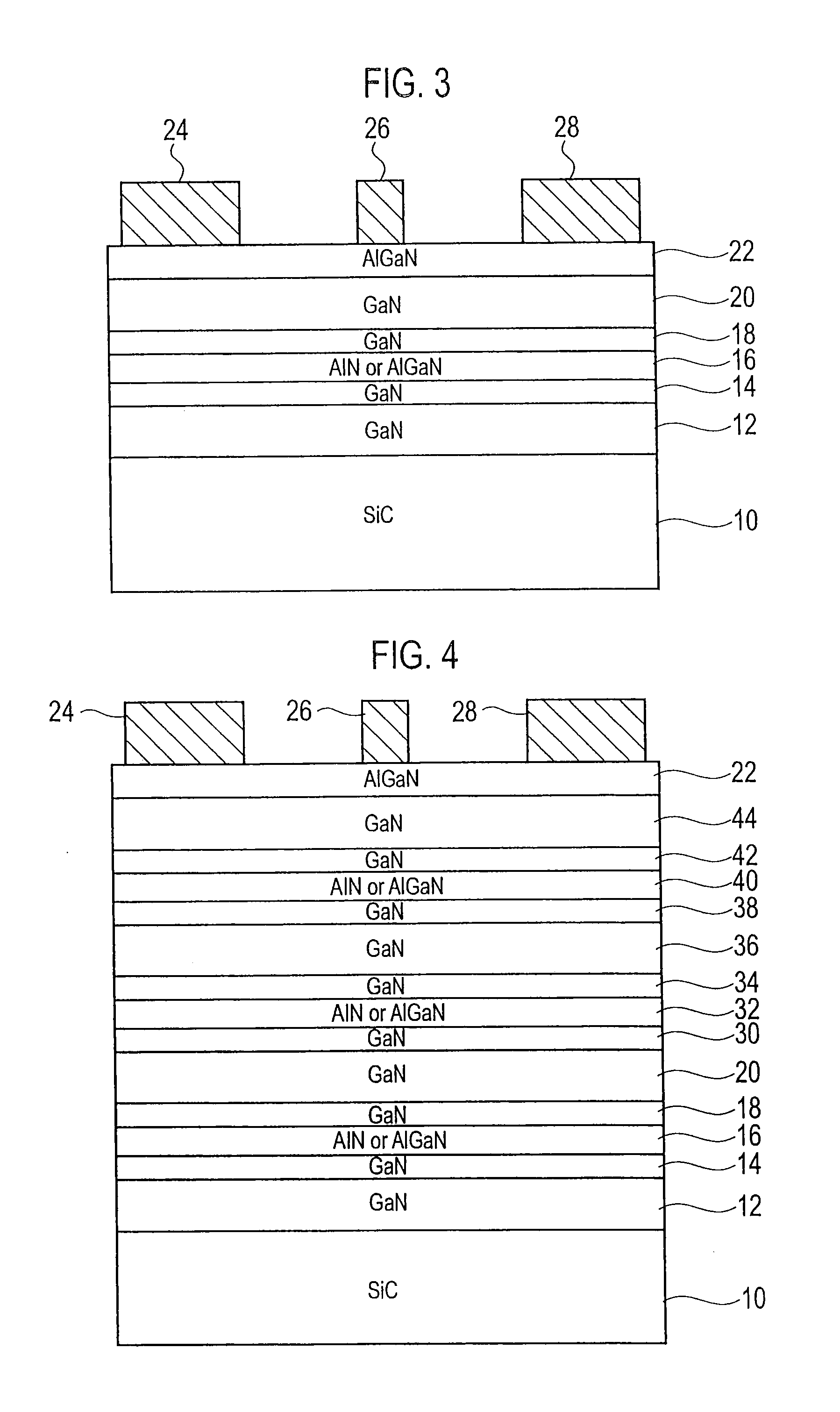
[0075]A semiconductor device according to the third embodiment of the present invention includes the layered structure (14, 16, 18) in which the three-layered structure shown in FIG. 2 is formed repeatedly multiple times. The three-layered structure is composed of the nitride based compound semiconductor layer 14 doped with the first transition metal atom, the aluminum gallium nitride layer (AlxGa1-xN) (where 0.116 placed on the nitride based compound semiconductor layer 14, and the nitride based compound semiconductor layer 18 placed on the aluminum gallium nitride layer (AlxGa1-xN) (where 0.116 and doped with the second transition metal atom.

[0076]That is, the semiconductor device according to the third embodiment of the present invention includes: the substrate 10; the layered structure (14, 16, 18) which is placed on the substrate 10 and in which the three-layered structure is formed repeatedly multiple times (for example, about 2 to 3 times); the aluminum gall...


PUM

PropertyMeasurementUnit
sizeaaaaaaaaaa
thicknessaaaaaaaaaa
thicknessaaaaaaaaaa

Abstract

A semiconductor device and a fabrication method of the semiconductor device, the semiconductor device including: a substrate; a nitride based compound semiconductor layer placed on the substrate and doped with a first transition metal atom; an aluminum gallium nitride layer (AlxGa1-xN) (where 0.1<=x<=1) placed on the nitride based compound semiconductor layer; a nitride based compound semiconductor layer placed on the aluminum gallium nitride layer (AlxGa1-xN) (where 0.1<=x<=1) and doped with a second transition metal atom; an aluminum gallium nitride layer (AlyGa1-yN) (where 0.1<=y<=1) placed on the nitride based compound semiconductor layer doped with the second transition metal atom; and a gate electrode, a source electrode, and a drain electrode which are placed on the aluminum gallium nitride layer (AlyGa1-yN) (where 0.1<=y<=1). Accordingly, piezo charge is inactivated, leakage current and current collapse are reduced, high frequency characteristics can be improved by obtaining a high resistivity semiconductor layer, and stable high frequency performance can be obtained.

Description

CROSS REFERENCE TO RELATED APPLICATION AND INCORPORATION BY REFERENCE[0001]This application is based upon and claims the benefit of priority from prior Japanese Patent Application No. P2008-013720 filed on Jan. 24, 2008, the entire contents of which are incorporated herein by reference.BACKGROUND OF THE INVENTION[0002]1. Field of the Invention[0003]The present invention relates to a semiconductor device and a fabrication method of the semiconductor device. In particular, the present invention relates to a GaN (gallium nitride) related high power semiconductor device for obtaining stabilized high frequency performance, and a fabrication method of the semiconductor device.[0004]2. Description of the Related Art[0005]It is known that FETs (Field Effect Transistors) using a GaN (gallium nitride) related semiconductor have a large amount of current collapse and have a large amount of leakage current. As one of the cause, crystal dislocations and crystal defects in an epitaxial crystal ar...

Claims


Application Information

Patent Timeline
Patent Type & Authority Applications(United States)
IPC IPC(8): H01L29/778H01L21/338
CPCH01L29/1029H01L29/7785H01L29/207H01L29/2003
Inventor MATSUSHITA, KEIICHI
Owner KK TOSHIBA
Why Eureka
Try Eureka