Semiconductor device using element isolation region of trench isolation structure and manufacturing method thereof

a technology of isolation structure and element, which is applied in the direction of semiconductor devices, basic electric elements, electrical equipment, etc., can solve the problems of increasing the difficulty of filling the dielectric film, increasing the difficulty of forming the element isolation region, and raising the technical difficulty

Inactive Publication Date: 2009-08-06
KK TOSHIBA
View PDF12 Cites 205 Cited by
  • Summary
  • Abstract
  • Description
  • Claims
  • Application Information

AI Technical Summary

Benefits of technology

[0021]According to still another aspect of this invention, there is provided a semiconductor device that includes memory cells each having a gate dielectric film, charge storage layer, inter-polysilicon gate dielectric film and control gate stacked and formed on a semiconductor substrate, an element isolation region of a trench isolation structure formed on the semiconductor substra...

Problems solved by technology

Recently, logic devices whose gate width is less than 45 nm and flash memories whose half pitch is less than 50 nm are produced on a mass-production basis, which raises the technical difficulty.
It therefore becomes more important to further shrink the element isolation region, but, at the same time, it rapidly becomes more difficult to form the element isolation region as the downsizing is further advanced.
Therefore, the aspect ratio of an isolation trench in which a dielectric film is filled becomes higher for each generation of downsizing, thus rapidly increasing the difficulty in filling the dielectric film.
Particularly, since the aspect ratio is set to 3 or more in the generation after the generation of 0.1 μm, in a process performed for filling a silicon oxide film formed by a high density plasma-CVD (HDP-CVD) method and used, at present, as a standard technique for filling a dielectric film into an isolation trench, it becomes extremely difficult to perform the filling process without causing any voids (non-filled portions).
Since the SOD film shrinks in the heating process, the tensile stress accordingly increases, and crystalline defects caused by dislocation tend to occur in the semiconductor substrate.
Particularly, when the above method is applied to a flash memory in which a gate dielectric film is formed in advance, the following problem occurs.
First, sin...

Method used


Image

  • Semiconductor device using element isolation region of trench isolation structure and manufacturing method thereof
  • Semiconductor device using element isolation region of trench isolation structure and manufacturing method thereof
  • Semiconductor device using element isolation region of trench isolation structure and manufacturing method thereof

Examples


first embodiment

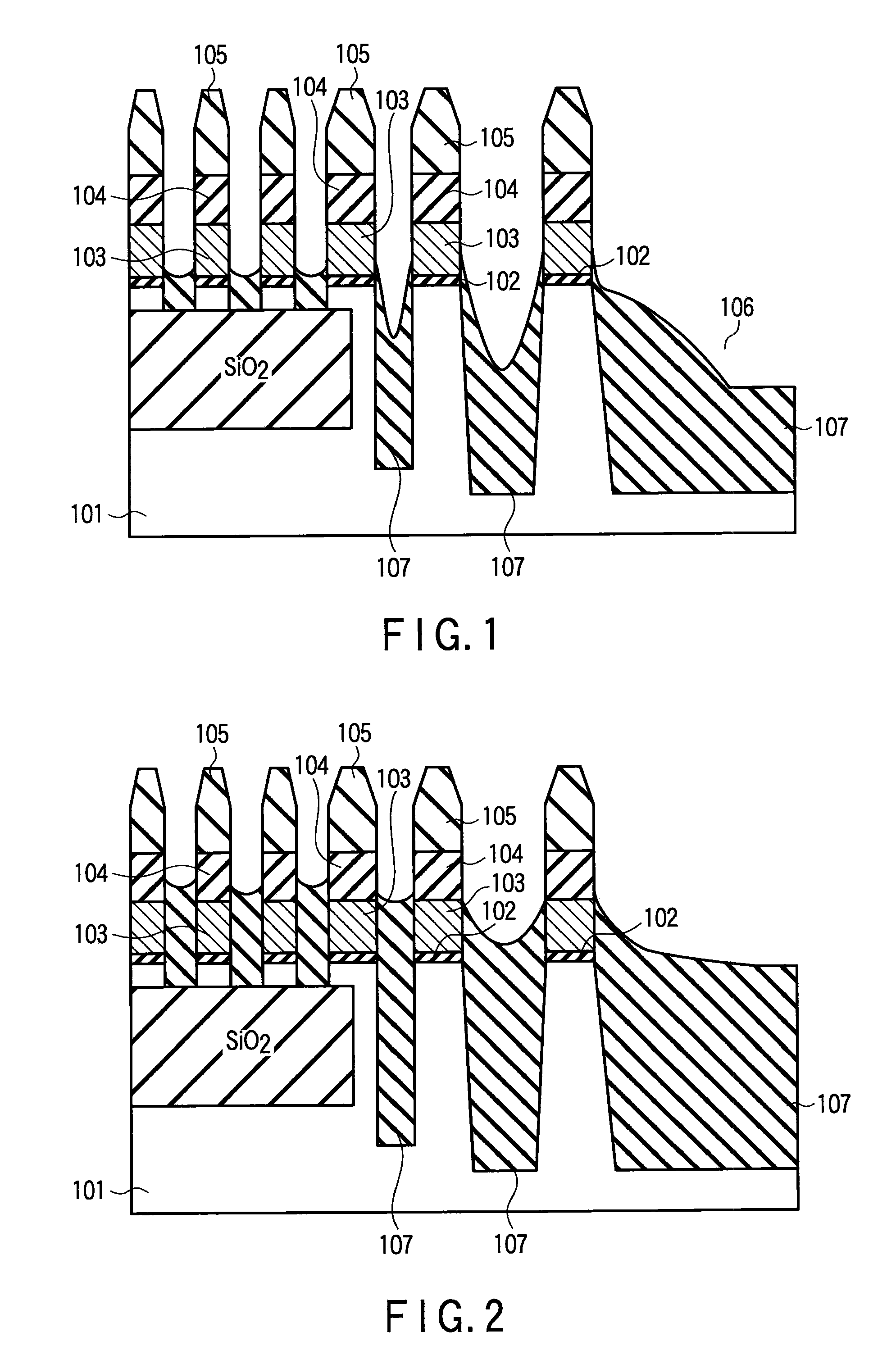
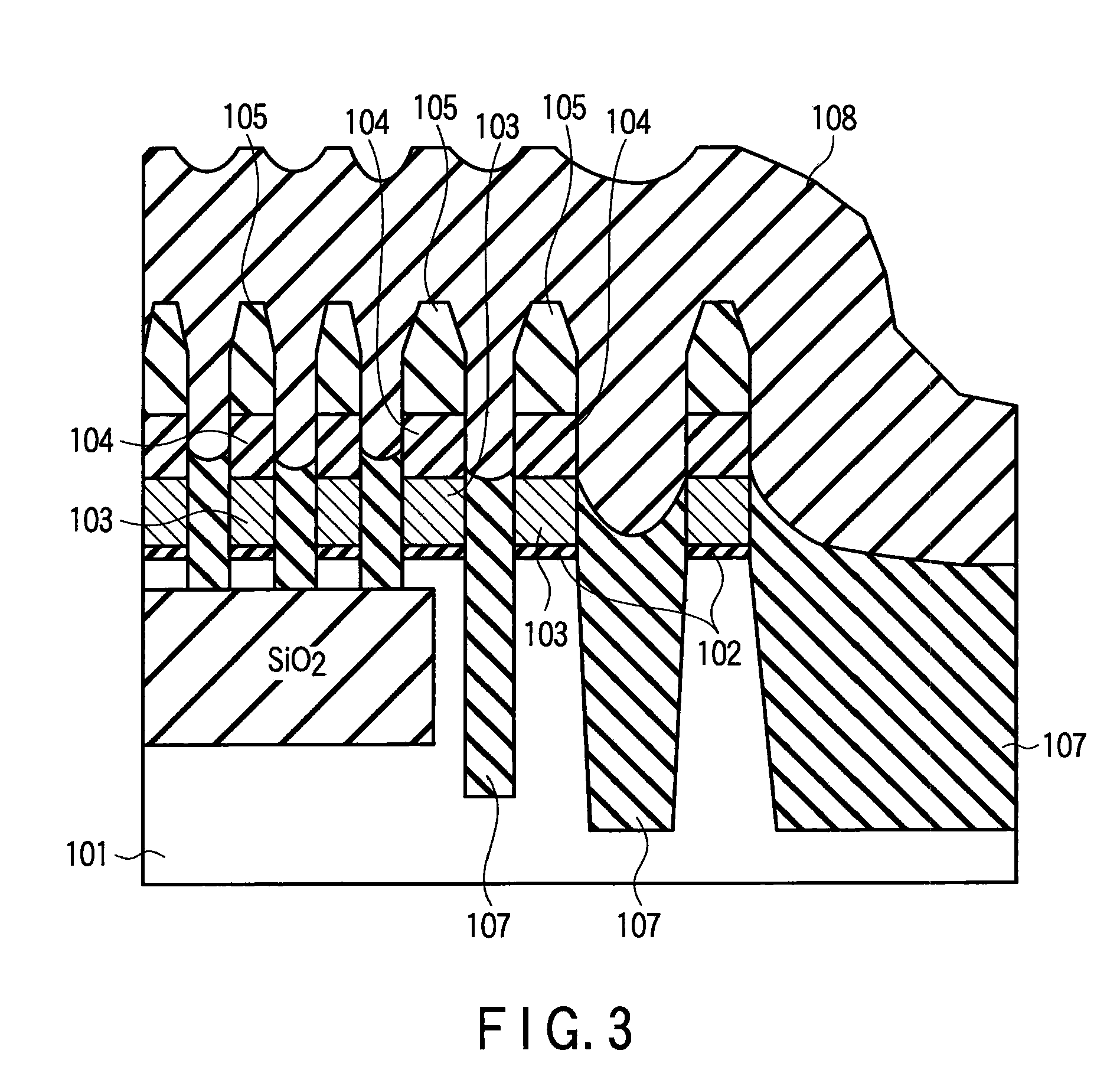
[0044]A semiconductor device and a manufacturing method thereof according to the first embodiment of this invention are explained with reference to FIGS. 1 to 7. This embodiment is an example in which a floating gate flash memory is formed on a partial SOI substrate, an O3-TEOS film having high underlying material selectivity is formed as the first dielectric film in an isolation trench for formation of an element isolation region and then an O3-TEOS film having no underlying material selectivity is filled therein as the second dielectric film.

[0045]According to the above system, a narrow STI portion in a cell portion is filled into a bottom-up with respect to the STI bottom portion without causing any seam. Therefore, the seam portion of the O3-TEOS film is etched in the wet etching step performed after formation of the STI portion and a lowering in the breakdown voltage of the cell portion can be suppressed. On the other hand, since the wide STI portion in the peripheral circuit p...

second embodiment

[0061]A semiconductor device and a manufacturing method thereof according to the second embodiment of this invention are explained with reference to FIGS. 9 to 12. Unlike the first embodiment, the present embodiment is an example in which an STI region is filled with an O3-TEOS film having high underlying material selectivity, and a perhydropolysilazane film, which is a type of SOG film in a floating gate flash memory using a bulk silicon substrate. In this embodiment, an O3-TEOS film is filled into a narrow STI portion in which the film quality of the SOG film tends to be degraded and a hybrid film of an SOG film and O3-TEOS film is filled into a wide STI portion in which a preferable film quality can be easily attained even if an SOG film is used.

[0062]Thus, in the case of the O3-TEOS film having high underlying material selectivity, a portion of the O3-TEOS film whose shape is inversely tapered after filling may occur due to the influence of the undercoat state, but occurrence of...

third embodiment

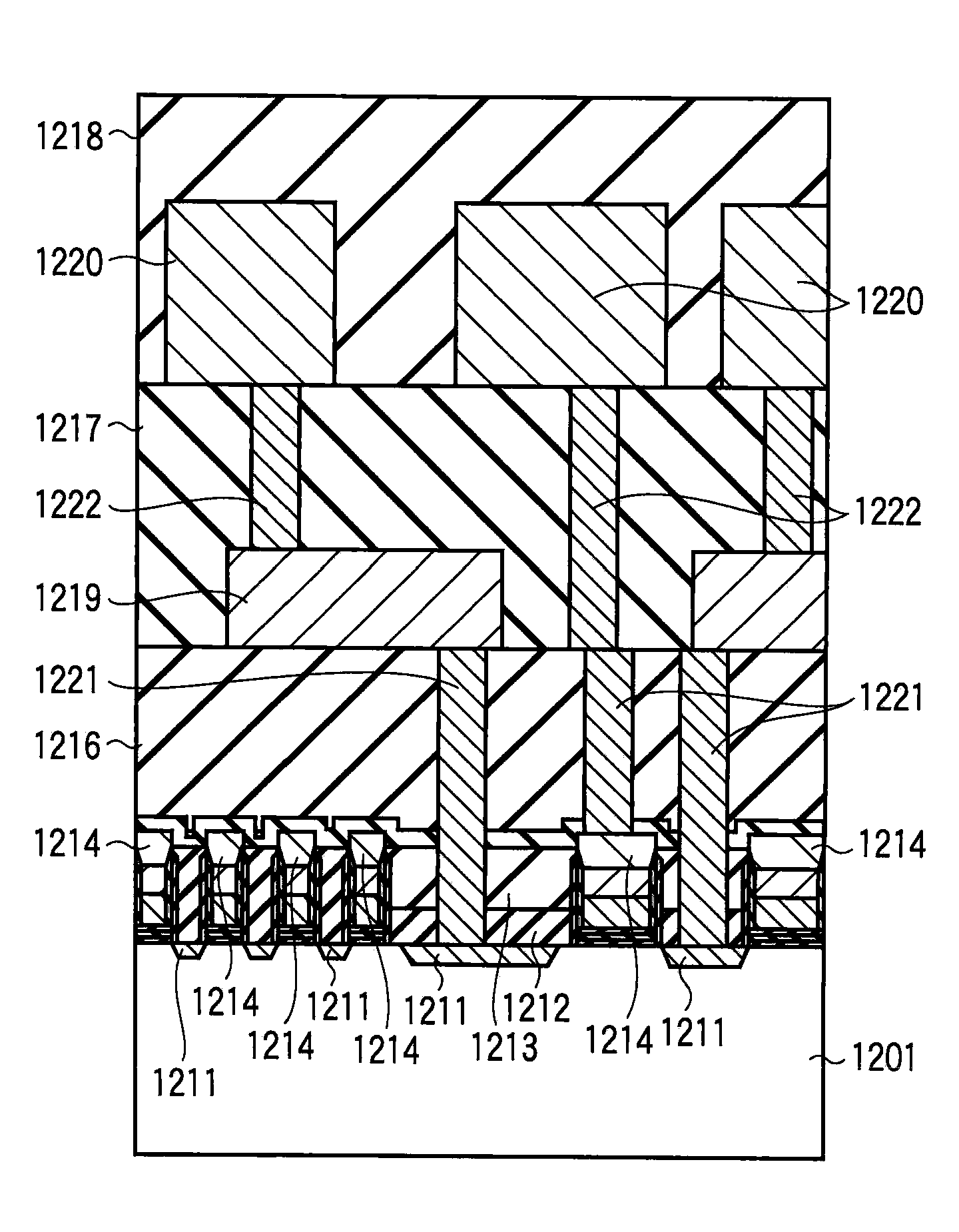
[0074]A semiconductor device and a manufacturing method thereof according to a third embodiment of this invention are explained with reference to FIGS. 13 to 17. This embodiment is an example applied to a charge trap flash memory formed on a partial SOI substrate. In this embodiment, a cell portion of the flash memory is filled with an O3-TEOS film having high underlying material selectivity in a liner form, a wide STI portion of the peripheral circuit portion is filled in a bottom-up form and the STI portion is completely filled by using the film in combination with the SOG film. As is explained in the second embodiment, it is possible to attain the effect that fixed charges and stress can be alleviated by reducing the coating film thickness of the SOG film due to formation of the wide STI portion in the bottom-up form.

[0075]As shown in FIG. 13, a silicon thermal oxynitride film 302 with a thickness of 4 nm used as gate dielectric films, a silicon nitride film 303 with a thickness ...


PUM


Abstract

A stacked film including a gate dielectric film and electrode film of each memory cell of a flash memory is formed on a semiconductor substrate. The stacked film is patterned by reactive ion etching to form an isolation trench for formation of an element isolation region and the surface of the semiconductor substrate is exposed to the internal portion of the isolation trench. An O3-TEOS film exhibiting underlying material selectivity during the deposition is formed in the isolation trench as the first filling dielectric film and then the isolation trench is filled with the second filling dielectric film to form an element isolation region of an STI structure.

Description

CROSS-REFERENCE TO RELATED APPLICATIONS[0001]This application is based upon and claims the benefit of priority from prior Japanese Patent Applications No. 2008-021892, filed Jan. 31, 2008; No. 2008-021999, filed Jan. 31, 2008; and No. 2008-201871, filed Aug. 5, 2008, the entire contents of all of which are incorporated herein by reference.BACKGROUND OF THE INVENTION[0002]1. Field of the Invention[0003]This invention relates to a semiconductor device using an element isolation region of a trench isolation structure and a manufacturing method thereof, which is applied to a flash memory and a flash memory manufacturing method, for example.[0004]2. Description of the Related Art[0005]Downsizing of LSIs is currently being advanced in order to enhance the performance of elements (enhance the operation speed and lower the power consumption) and suppress the manufacturing cost by increasing the elements density. Recently, logic devices whose gate width is less than 45 nm and flash memories ...

Claims


Application Information

Patent Timeline
IPC IPC(8): H01L29/792H01L21/762H01L29/06
CPCH01L21/76229H01L21/84H01L27/105H01L27/11526H01L27/1207H01L27/11573H01L27/11575H01L27/1203H01L29/42336H01L27/11529H10B41/41H10B41/40H10B43/50H10B43/40H10B41/35
Inventor KIYOTOSHI, MASAHIROKUBOTA, HIROSHI
Owner KK TOSHIBA
Why Eureka
Try Eureka