Impurity-activating thermal process method and thermal process apparatus

a technology of impurity activation and thermal process, which is applied in the direction of lighting and heating apparatus, ovens, furnaces, etc., can solve the problems of short thermal process time, ineffectiveness, and similar millisecond annealing performed at the same time, so as to improve the activation rate of impurity, reduce the resistance of the source/drain region, and increase the diffusion length or inactivation of impurity

Inactive Publication Date: 2009-08-06
PANASONIC CORP
View PDF6 Cites 15 Cited by
  • Summary
  • Abstract
  • Description
  • Claims
  • Application Information

AI Technical Summary

Benefits of technology

[0029]As described above, according to the present invention, it is possible to improve the impurity activation rate without thermally damaging, for example, the silicon substrate, the pattern formed thereon, the interface therebetween, etc., and without increasing the impurity diffusion length or inactivating the impurity. Therefore, it is possible to reduce the resistance of the source/drain region and that of the extension region in the transis

Problems solved by technology

This is because millisecond annealing performed at a similar temperature to that of spike RTA, e.g., about 1100° C., will not be effective with the short thermal process time.
In view of this, millisecond annealing is sometimes performed at a thermal process temperature of a sub-melt region close to the silicon melting temperature (1412° C.) such as about 1300 t

Method used


Image

  • Impurity-activating thermal process method and thermal process apparatus
  • Impurity-activating thermal process method and thermal process apparatus
  • Impurity-activating thermal process method and thermal process apparatus

Examples


first embodiment

[0045]An impurity-activating thermal process method according to a first embodiment of the present invention will now be described with reference to the drawings.

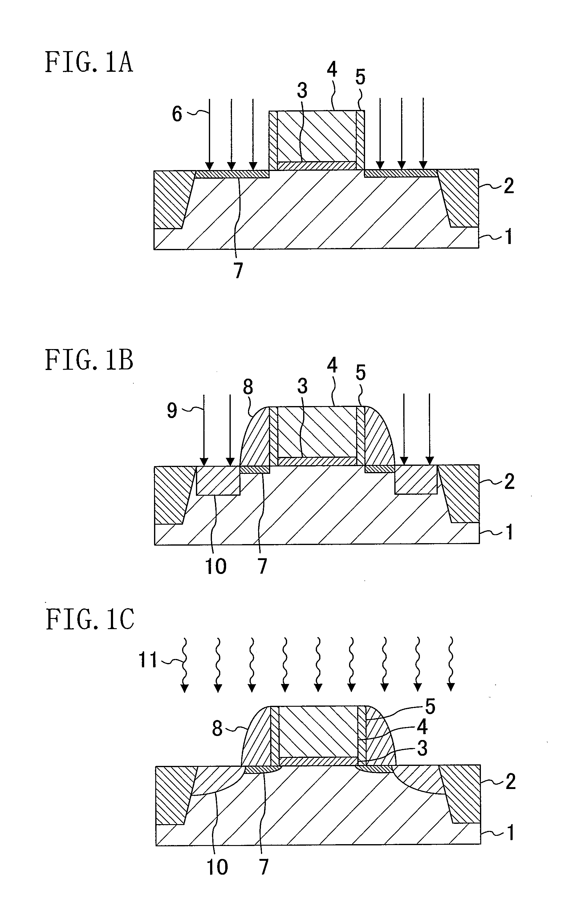
[0046]FIGS. 1A to 1C are cross-sectional views each showing a step of a method for manufacturing a semiconductor device based on an impurity-activating thermal process method of the present embodiment, more specifically a method for forming a MOS (metal-oxide-semiconductor) transistor using millisecond annealing for impurity activation.

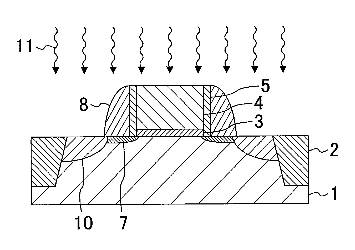
[0047]First, as shown in FIG. 1A, an isolation region 2 is formed on a silicon substrate 1, and an impurity is introduced into the silicon substrate 1 for threshold control, after which a gate electrode 4 is formed on the silicon substrate 1 with a gate insulating film 3 interposed therebetween. Then, after an offset spacer 5 is formed on the sidewall of the gate electrode 4, the silicon substrate 1 is subjected to an impurity ion implantation 6 using the gate electrode 4 and the offset space...

second embodiment

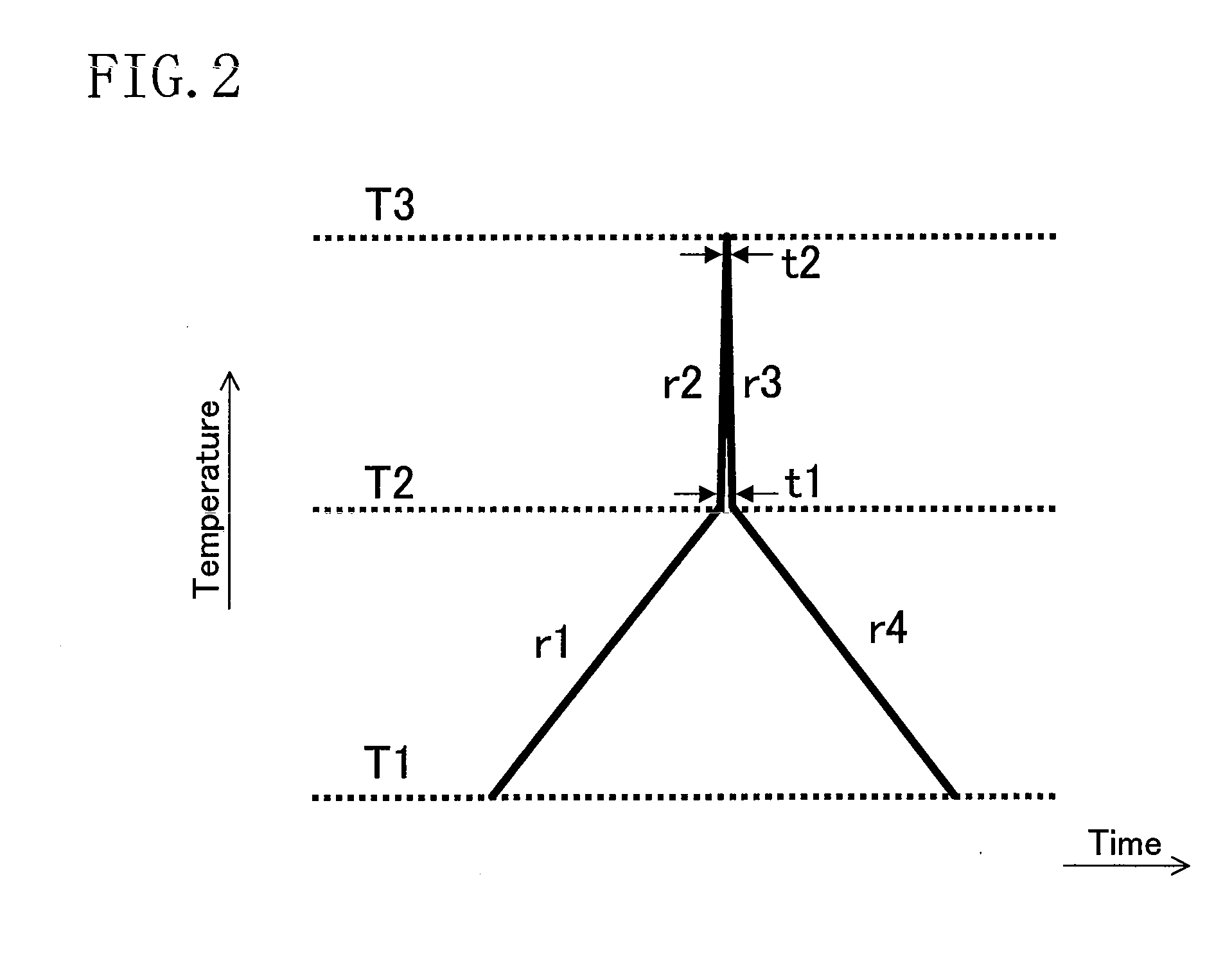
[0070]An impurity-activating thermal process method according to a second embodiment of the present invention will now be described with reference to the drawings. The method of manufacturing a semiconductor device using the impurity-activating thermal process method of the present embodiment, more specifically steps of a method for forming a MOS transistor using millisecond annealing for impurity activation, are the same as those of the first embodiment shown in FIGS. 1A to 1C. Specifically, an impurity is introduced into the silicon substrate 1 to form the extension region 7 and the source / drain region 10, and then the impurity-activating thermal process method of the present embodiment is performed. The impurity-activating thermal process method of the present embodiment will now be described in detail. FIG. 5 shows an example of a temperature sequence in the impurity-activating thermal process method of the present embodiment.

[0071]First, as in the first embodiment, the temperat...

third embodiment

Variation of Third Embodiment

[0111]A thermal process apparatus according to a variation of the third embodiment of the present invention, more specifically a thermal process apparatus for carrying out the impurity-activating thermal process method of the first and second embodiments, will now be described with reference to the drawings with respect to a case where a flash lamp (e.g., an Xe flash lamp) is used as the heat source.

[0112]FIG. 12A is a circuit diagram showing a general configuration of the thermal process apparatus of the present variation, and FIG. 12B illustrates an operation thereof. The present variation is different from the third embodiment shown in FIG. 11A in the configuration of a circuit to which the second group of flash lamps 52 are connected. Referring to FIG. 12A, in the circuit to which the second group of flash lamps 52 are connected in the present variation, the circuit portion including a plurality (N) of condensers C1, C2, . . . , Cn and the second gro...


PUM


Abstract

An impurity-activating thermal process is performed after a target is subjected to an impurity introduction step. In this thermal process, while a spike RTA process including a holding period for holding a temperature at a predetermined temperature is performed, at least one iteration of millisecond annealing at a temperature higher than the predetermined temperature is performed during the holding period of the spike RTA process.

Description

CROSS REFERENCE TO RELATED APPLICATION[0001]This application claims priority under 35 U.S.C. §119 on Patent Application No. 2008-26939 filed in Japan on Feb. 6, 2008, the entire contents of which are hereby incorporated by reference.BACKGROUND OF THE INVENTION[0002]1. Field of the Invention[0003]The present invention relates to a method for manufacturing a semiconductor device and, more particularly, to an impurity-activating thermal process method after impurity introduction, and a thermal process apparatus for carrying out the method.[0004]2. Description of the Background Art[0005]In recent years, devices have been downsized along with the increase in the degree of integration, functionality and speed of semiconductor integrated circuit devices. Accordingly, progress has been made not only with lateral miniaturization, e.g., a reduced gate length of a transistor, but also with vertical miniaturization, e.g., an ultra-thin gate insulating film. Particularly, in a transistor, the im...

Claims


Application Information

Patent Timeline
IPC IPC(8): H01L21/00A21B1/06H01L21/30H01L21/40
CPCH01L21/2686H01L21/324H01L29/7833H01L29/6659H01L21/67115
Inventor TAKAHASHI, KAZUMAYONEDA, KENJI
Owner PANASONIC CORP
Why Eureka
Try Eureka