Infrared-detecting element and infrared image sensor using the same

a technology of infrared sensor and infrared image, which is applied in the direction of thermoelectric devices, optical radiation measurement, instruments, etc., can solve the problems of difficult preparation of materials directly on silicon substrates for infrared sensors produced by cmos process, high crystallization temperature, and difficult ion etching

Inactive Publication Date: 2009-08-13
KK TOSHIBA
View PDF5 Cites 13 Cited by
  • Summary
  • Abstract
  • Description
  • Claims
  • Application Information

AI Technical Summary

Problems solved by technology

However, in these materials, crystallization temperature is high, and ion etching is difficult, and a precious-metal electrode material is required because the materials are oxides.
From such reasons, there is a problem that it is difficult to prepare the materials directly on a silicon substrate for an infrared sensor produced by CMOS process.
Accordingly, instead of the monolithic process of CMOS, a complicated expensive hybrid process using a bonding technique or the like cannot help being used.
However, the pyroelectric-type infrared-detecting element has had some problems.
The first problem is that the complicated steps of bonding and of dissolving and removing the substrate in the production of the detecting element become large obstacles in reliability, accuracy, microfabrication, and preparation of array.
The second problem is that an amplifier connected to the infrared-detecting element cannot help being provided on a different substrate from the substrate of the infrared-detecting element, and the infrared-detecting element and the amplifier come to be connected with interconnection.
Therefore, in comparison with the case that the infrared-detecting portion and the amplifier are formed in a lump on a single substrate only by a thin-film step, noise or the like easily enters therein and the detection accuracy deteriorates.
However, the largest problem of the bolometer-type infrared sensor is badness of detection sensitivity.
However, with respect to various noises such as Johnson noise contained in voltage generated in the resistance element, the voltage change amount generated by temperature change by infrared irradiation is small and therefore S / N ratio is bad and detection with good sensitivity is very difficult.
However, when such a material is film-formed on a silicon substrate, it is not easy to produce a single crystal film having sufficient piezoelectricity or a high orientational film.
However, because the band gap is narrow, leak current is necessarily very large and it involves very large difficulty to perform reading in room temperature.
As described above, every one of pyroelectric-type, bolometer-type, and pseudo-pyroelectric-effect-type infrared-detecting elements and infrared image sensors using the elements, which are conventional techniques, has problems.
However, every one of the attempts has both merits and demerits, and therefore, in the present situation, the above-described techniques has not been substituted.

Method used


Image

  • Infrared-detecting element and infrared image sensor using the same
  • Infrared-detecting element and infrared image sensor using the same
  • Infrared-detecting element and infrared image sensor using the same

Examples


first embodiment

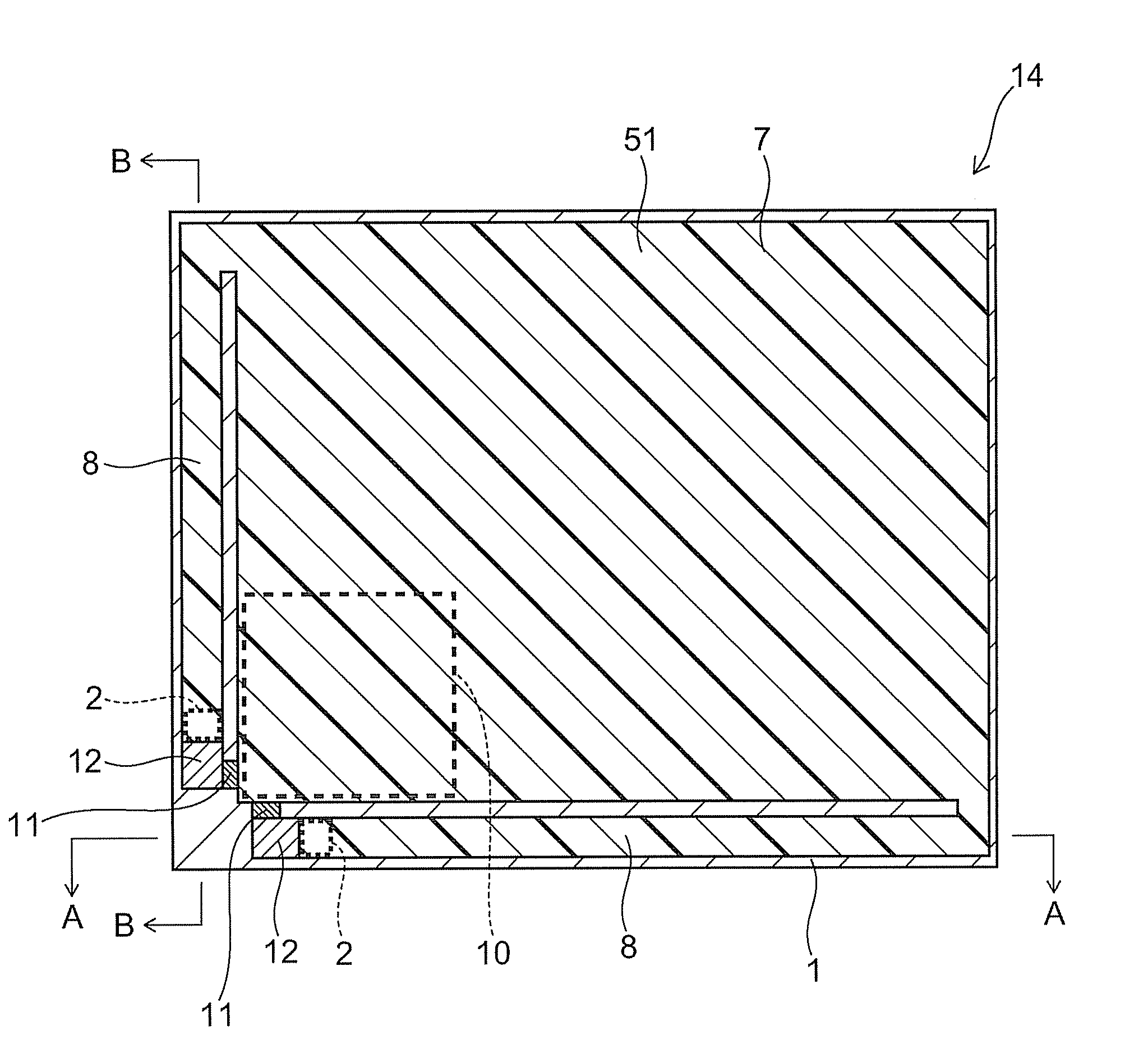
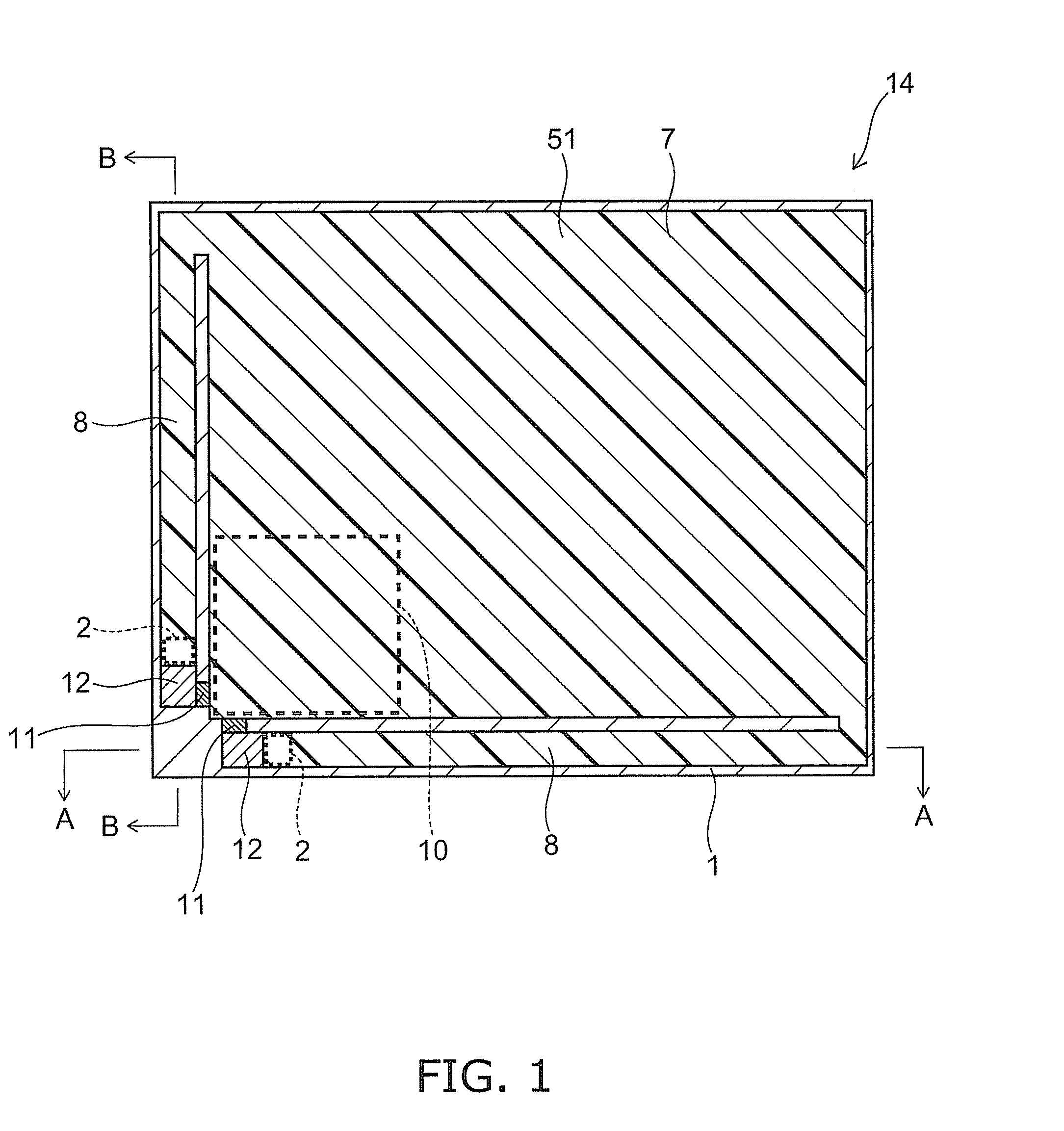
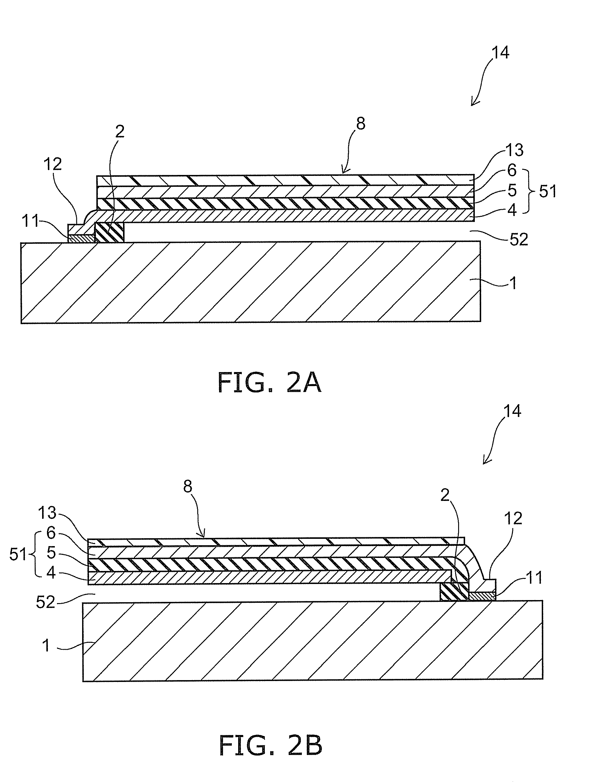
[0032]FIG. 1 is a plan view of an infrared-detecting element 14 according to a first embodiment. And, FIG. 2 is a partial section view of the infrared-detecting element according to the first embodiment, and FIGS. 2A and 2B are section views of A-A line and B-B line of FIG. 1, respectively.

[0033]As shown in FIGS. 1 and 2, an anchor 2 is formed on a substrate 1. A laminated body 51 is composed of a lower electrode 4, an upper electrode 6, and a piezoelectric film 5 sandwiched by the lower electrode 4 and the upper electrode 6. A connecting beam 8 that is an end of the laminated body 51 is coupled to the anchor 2, and the laminated body 51 is supported by the anchor 2 in the state with a gap 52 in an upper portion of the substrate 1. Moreover, amplifier 10 is formed on the substrate 1, and each of the lower electrode 4 and the upper electrode 6 is connected with a contact portion 12 to a interconnection 11 from the amplifier 10. Moreover, on the upper electrode 6, an infrared-absorbin...

second embodiment

[0078]Next, the infrared-detecting element according to a second embodiment of this invention will be explained.

[0079]FIG. 4 is a plan view of the infrared-detecting element 15 according to a second embodiment of this invention. Moreover, FIG. 5 is a section view of A-A section view. The laminated body 51 and the thermosensitive portion 7 have a cantilever beam structure for the first embodiment but have a center impeller beam structure for the second embodiment. The same numbers are appended to the components having the same roles as the first embodiment will be explained.

[0080]As shown in FIGS. 4 and 5, the anchors 2 are formed at two places on the substrate 1. The laminated body 51 is composed of the lower electrode 4, the upper electrode 6, and the piezoelectric film 5 sandwiched by the lower electrode 4 and the upper electrode 6. The portions of connecting beams 8 of right and left ends of the laminated body 51 are connected to the anchors 2, and the laminated body 51 is suppor...

third embodiment

[0100]Next, an infrared-detecting element of a third embodiment of this invention will be explained.

[0101]FIG. 8 is a circuit view showing a circuit structure of the infrared-detecting element according to the third embodiment. As shown in FIG. 8, in the infrared-detecting element 300 of the third embodiment, the amplifier 310 is connected to the laminated body 301, and includes a first transistor 303 for converting the charge generated in the laminated body 301 into voltage, a second transistor (load transistor) 302 connected to the first transistor 303, a first terminal 304 for applying voltage to a gate of the second transistor 302, a second terminal 305 for applying voltage to source of the second transistor 302, and a third terminal 306 for getting charge information from drain of the first transistor 303. As shown in FIG. 8, in the infrared-detecting element 300 of the third embodiment, the amplifier formed on the substrate has a circuit for converting information of charge ge...


PUM


Abstract

An infrared-detecting element includes: a substrate; a laminated body; an anchor coupling a part of the laminated body with the substrate and supporting the laminated body with a gap above the substrate; and an amplifier provided on the substrate and connected to at least one of the lower electrode and the upper electrode. The laminated body has a lower electrode, an upper electrode, and a piezoelectric film made of aluminum nitride which is provided between the lower electrode and the upper electrode and in which a c-axis is oriented almost perpendicularly to a film plane. The amplifier has a circuit performing conversion into voltage according to a charge generated in the laminated body.

Description

CROSS-REFERENCE TO RELATED APPLICATIONS[0001]This application is based upon and claims the benefit of priority from the prior Japanese Patent Application No. 2007-234696, filed on Sep. 10, 2007; the entire contents of which are incorporated herein by reference.BACKGROUND OF THE INVENTION[0002]1. Field of the Invention[0003]This invention relates to an infrared-detecting element using a piezoelectric film and to an infrared image sensor using the same.[0004]2. Background Art[0005]All of infrared-detecting elements used generally for consumers are uncooled-type infrared-detecting elements and classified roughly to pyroelectric type and bolometer type.[0006]In a pyroelectric-type infrared sensor, it is necessary that a special material called as pyroelectric body is used as the infrared-detecting element. Representatively, a material of a lead titanate or a barium titanate, which are ferroelectric materials of oxide, is used. However, in these materials, crystallization temperature is ...

Claims


Application Information

Patent Timeline
Patent Type & Authority Applications(United States)
IPC IPC(8): H01L27/14
CPCG01J5/02G01J5/023H01L37/00G01J5/34G01J5/40G01J5/024H10N15/00
Inventor KAWAKUBO, TAKASHINISHIGAKI, MICHIHIKONAGANO, TOSHIHIKOIIDA, YOSHINORIFUJIWARA, IKUOHONDA, HIROTO
Owner KK TOSHIBA
Why Eureka
Try Eureka