Inspection apparatus
a technology of inspection apparatus and inspection chamber, which is applied in the field of inspection apparatus, can solve the problems of improving throughput, difficult to use refractive optics, and difficult to use in the wide wavelength band of first related art, and achieves the effects of simplifying optics, high throughput and high sensitivity inspection, and reducing the number of optical elements
- Summary
- Abstract
- Description
- Claims
- Application Information
AI Technical Summary
Benefits of technology
Problems solved by technology
Method used
Image
Examples
embodiment 1
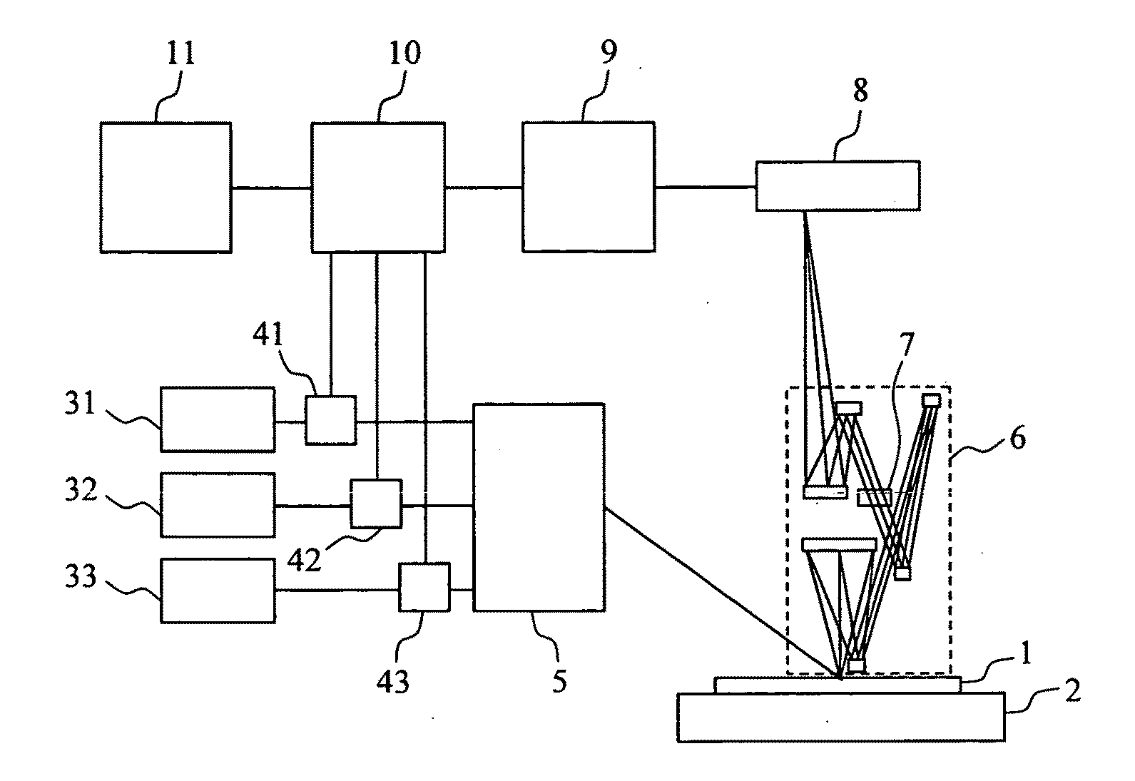
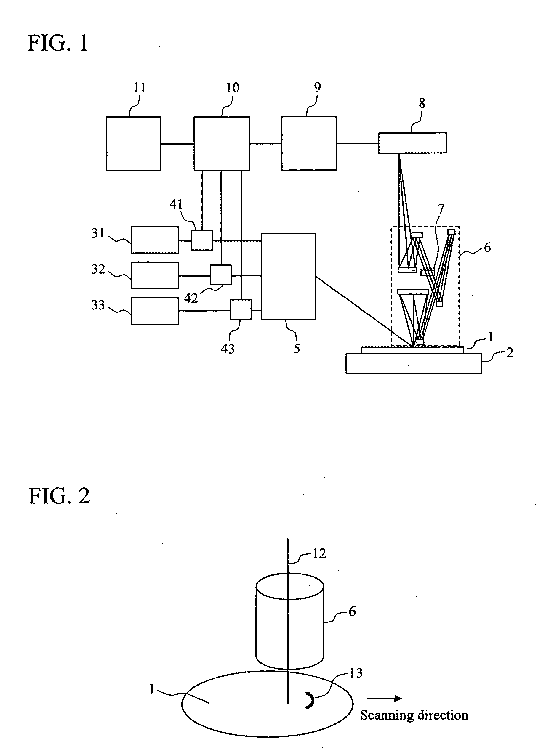
[0073]A dark-field inspection apparatus for inspecting a semiconductor wafer will be described as an embodiment of the present invention. FIG. 1 schematically shows the construction of the inspection apparatus. Main components of the apparatus are a stage 2 on which a wafer 1 is mounted, a visible light laser 31, an ultraviolet laser 32, a deep ultraviolet laser 33, attenuators 41, 42, and 43, an illumination optics 5, a reflective optics 6, a spatial filter 7, an image sensor 8, an image processing system 9, a control system 10, and an input-output operation system 11.
[0074]When the wafer 1 is loaded in the inspection apparatus, an operator inputs information on the manufacturing process and a defect of interest to the input-output operation system 11. The control system 10 selects an optimum wavelength band such as described below by using this information and referring to a database accumulated in advance through a simulation or an experiment. The lasers 31, 32, and 33 emit light...
embodiment 2
[0092]An embodiment of the present invention preferable in a case where a plurality of defects of interest exist on a wafer will be described with reference to FIG. 6. The same reference numerals as those in FIG. 1 denote identical or corresponding components. In this embodiment, diffractive-optical elements 16 are disposed on the exit side of the reflective optics 6 to separate light into wavelength bands. As each diffractive-optical element, a diffraction grating, a prism or the like can be used. Separated light is imaged on an image sensor 81 and an image sensor 82 in correspondence with the wavelength bands. An optimum wavelength band can be selected with respect to each detect of interest. Therefore, an image of a high signal-to-noise ratio can be obtained.
embodiment 3
[0093]Another embodiment of the present invention will be described with reference to FIG. 7. The same reference numerals as those in FIG. 1 denote identical or corresponding components. In this embodiment, a lamp 17 which emits light in a wide wavelength band from a visible light region to a deep ultraviolet region is used as a light source, and a wavelength filter 18 allows light in a predetermined wavelength band to pass through. The lamp has a lower output per wavelength band in comparison with lasers but is capable of making finer selections from wavelength bands because it emits a continuous spectrum of light. Finer selections from wavelength bands can be made in the wavelength filter 18 on the basis of a command from the control system 10. The present embodiment is highly effective in reducing the bad influence of thin-film interference. Also, the construction of the apparatus is simplified in comparison with a case where a plurality of lasers are incorporated.
PUM
 Abstract
Description
Claims
Application Information


