Electro-Optical Modulator Structure

a technology of optical modulator and structure, applied in the field of electro-optical modulator structure, can solve the problems of difficult to predict the charge distribution, difficult to perform analytical calculations on the concentration of free carriers that are injected to a soi-based device, etc., and achieve the effects of improving the performance of electro-optical modulators, reducing fabrication costs, and reducing siz

Inactive Publication Date: 2009-09-03
RAMOT AT TEL AVIV UNIV LTD
View PDF5 Cites 23 Cited by
  • Summary
  • Abstract
  • Description
  • Claims
  • Application Information

AI Technical Summary

Benefits of technology

[0021]There is a need in the art to improve the performance of electro-optical (EO) modulators, by reducing their size, reducing fabrication costs, increasing modulation depth and speed, and reducing supply power. The present invention combines all of these requirements by providing an ultra-compact optical modulator comprising at least one resonator on a semiconductor chip....

Problems solved by technology

Performing analytical calculation of the concentration of free carriers that are injected to a SOI-based device is rather difficult.
The major obstacle in such a process is the surface recombination which h...

Method used


Image

  • Electro-Optical Modulator Structure
  • Electro-Optical Modulator Structure
  • Electro-Optical Modulator Structure

Examples


Embodiment Construction

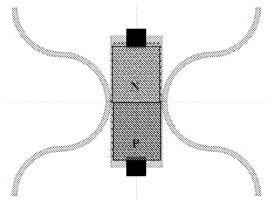
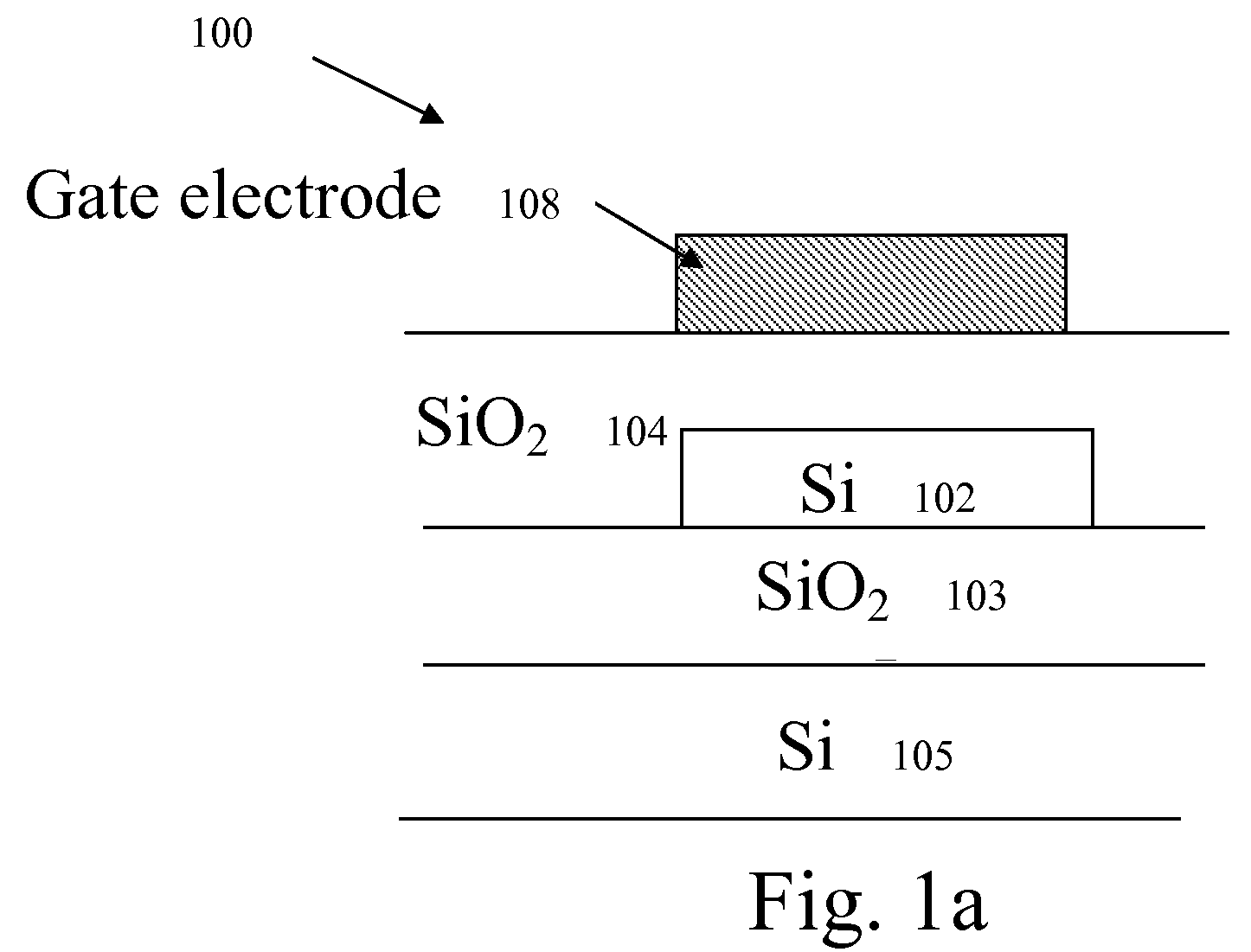
[0067]The present invention provides a novel high performance EO modulator for modulating incoming light having a certain wavelength range i.e. a wavelength of operation. Reference is made to FIG. 1a, generally illustrating a cross-sectional view of the layer structure forming the modulator of the present invention. To facilitate understanding, the same reference numbers are used for identifying components that are common in all the examples.

[0068]In this non-limiting example, the EO modulator structure 100 can be fabricated on a SOI wafer with the following characteristics: 230 nm thick resonator (c-Si) layer 102, 3 μm thick buffer (SiO2) layer 103 and a ˜500 μm thick handle (c-Si) layer 105. The top silicon layer 102 deposited on the SiO2 103 is recovered by another SiO2 buffer layer 104, which constitutes the cladding of a ridge waveguide (450 nm wide) that guides light in and out of the SOI chip. The resonator is located on the modulator layer inside the ridge waveguide. On top ...


PUM


Abstract

The present invention discloses an ultra-compact optical modulator comprising at least one resonator on a semiconductor chip. The EO modulator modulates incoming light having a certain wavelength range and comprises a waveguide layer accommodating at least one resonator having a periodic complex refraction index distribution structure defining a periodic defect band-edge and a cladding layer; and at least one electrode; the waveguide layer, the cladding layer and the electrode forming a capacitor structure; such that when an external voltage is applied to the capacitor structure the free carrier concentration in the waveguide layer is controlled, enabling a modulation of the resonator's refractive index; wherein the periodic defect band-edge is selected to be within the wavelength range, enabling a slow-light propagation of the incoming light within the waveguide layer.

Description

RELATED APPLICATIONS[0001]This application claims the benefit under 35 USC 119(e) of U.S. Provisional Application Nos. 61 / 033,177 filed on Mar. 3, 2008, and 61 / 040,987 filed on Mar. 31, 2008, both of which are incorporated herein by reference in their entirety.FIELD OF THE INVENTION[0002]The present invention relates generally to an electro-optical modulator structure and to different applications using the electro-optical modulator.BACKGROUND OF THE INVENTION[0003]The following references are considered to be pertinent for the purpose of understanding the background of the present invention:[0004][1] G. Muller, M. Muller, A. Wicht, R. H. Rinkleff, and K. Danzmann, “Optical resonator with steep internal dispersion,” Phys. Rev. A 56, 2385-2389 (1997).[0005][2] M. Soljacic, E. Lidorikis, L. Vestergaard Hau, J. D. Joannopoulus, “Enhancement of microcavities lifetime using highly dispersive materials,” Phys. Review E. 71, 026602 (2005).[0006][3] Damian Goldring, Uriel Levy and David Men...

Claims


Application Information

Patent Timeline
IPC IPC(8): G02F1/035G02B6/00
CPCB82Y20/00G02B6/12007G02F1/011G02F1/025G01N21/7746G02F2202/32G02F2203/15G02B2006/1213G02F2202/10
Inventor GOLDRING, DAMIANMENDLOVIC, DAVID
Owner RAMOT AT TEL AVIV UNIV LTD
Why Eureka
Try Eureka